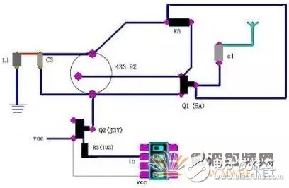
PCB design of the baseband circuit requires a lot of signal processing engineering knowledge. The transmitter's RF circuitry converts, upconverts, and upconverts the processed baseband signal into a designated channel and injects this signal into the transmission medium. Conversely, the receiver's RF circuit can take signals from the transmission medium and convert and down-convert them to the fundamental frequency.
Wireless transmitters and receivers are conceptually divided into two parts: the fundamental frequency and the radio frequency. The fundamental frequency contains the frequency range of the transmitter's input signal and also the frequency range of the receiver's output signal. The bandwidth of the fundamental frequency determines the basic rate at which data can flow through the system. The fundamental frequency is used to improve the reliability of the data stream and to reduce the load imposed by the transmitter on the transmission medium below a specific data transmission rate.
First, the transmitter has two main PCB design goals
The first is that they must transmit a specific amount of power as much as possible while consuming the least amount of power.
The second is that they cannot interfere with the normal operation of the transceivers in adjacent channels.
As far as the receiver is concerned, there are three main PCB design goals: first, they must accurately restore small signals; second, they must be able to remove interfering signals outside the desired channel; the last point, like the transmitter, they must consume the power Very small.

Second, the large interference signal of the RF circuit simulation
The receiver must be sensitive to small signals, even when large interfering signals (barriers) are present. This occurs when an attempt is made to receive a weak or long-range transmit signal, with a powerful transmitter nearby broadcasting in an adjacent channel. The interference signal may be 60~70 dB larger than the expected signal, and may block the reception of the normal signal by a large amount of coverage in the input phase of the receiver or by causing the receiver to generate excessive noise during the input phase. If the receiver is in the input phase and the interferer drives the non-linear region, the above two problems will occur. To avoid these problems, the front end of the receiver must be very linear.
Therefore, "linear" is also an important consideration when designing a receiver for a PCB. Since the receiver is a narrowband circuit, the nonlinearity is measured by measuring "intermodula distortion". This involves using two sine or cosine waves of similar frequency and located in the center band to drive the input signal and then measure the product of its alternating modulation. In general, SPICE is a time-consuming and costly simulation software because it has to perform many loop operations to get the required frequency resolution to understand the distortion.
Third, the expected signal of the RF circuit simulation
The receiver must be sensitive to detect small input signals. In general, the receiver's input power can be as small as 1 μV. The sensitivity of the receiver is limited by the noise generated by its input circuitry. Therefore, noise is an important consideration when designing a receiver for a PCB. Moreover, the ability to predict noise with simulation tools is indispensable. Figure 1 is a typical superheterodyne receiver. The received signal is filtered first and then amplified by a low noise amplifier (LNA). This signal is then mixed with this signal using the first local oscillator (LO) to convert this signal to an intermediate frequency (IF). The noise performance of the front-end circuitry is primarily dependent on the LNA, mixer, and LO. Although the noise of the LNA can be found using conventional SPICE noise analysis, it is useless for the mixer and LO because the noise in these blocks is severely affected by the large LO signal.
A small input signal requires the receiver to have a very large amplification function, which typically requires a gain of 120 dB. At such high gains, any signal that is coupled back to the input from the output can cause problems. An important reason for using a superheterodyne receiver architecture is that it distributes the gain across several frequencies to reduce the probability of coupling. This also makes the frequency of the first LO different from the frequency of the input signal, preventing large interfering signals from "contaminating" to small input signals.
For some different reasons, in some wireless communication systems, a direct conversion or homodyne architecture can replace the superheterodyne architecture. In this architecture, the RF input signal is directly converted to the fundamental frequency in a single step, so most of the gain is in the fundamental frequency and the LO is the same frequency as the input signal. In this case, the influence of a small amount of coupling must be known, and a detailed model of the "stray signal path" must be established, such as coupling through the substrate, package pins and bond wires. Coupling between (bondwire) and coupling through the power line.
Fourth, the interference of adjacent channels of RF circuit simulation
Distortion also plays an important role in the transmitter. The non-linearity produced by the transmitter in the output circuit may spread the bandwidth of the transmitted signal in adjacent channels. This phenomenon is called "spectral regrowth." Before the signal reaches the power amplifier (PA) of the transmitter, its bandwidth is limited; however, the "intermodulation distortion" in the PA causes the bandwidth to increase again. If the bandwidth is increased too much, the transmitter will not be able to meet the power requirements of its neighboring channels. When transmitting a digital modulation signal, in fact, SPICE cannot be used to predict the re-growth of the spectrum. Since approximately 1000 digital symbol transfer operations must be simulated to obtain a representative spectrum and also need to be combined with high frequency carriers, these will make SPICE transient analysis impractical.
- The Description of wifi Antenna
-
When selecting the antenna, it is necessary to pay attention to whether the Connector of the antenna matches the connector of the connected device. Generally, SMA and TNC are used for WIFI
To use on the router, but on the 2.4 G wireless monitoring equipment fittings, if match, also can achieve the enhancement effect of the wireless signal transmission Magnetic antenna base, can suck on metal surfaces, makes the antenna signal is stronger Plug and play, without any additional conditions, but the antenna gain and directional property management are key points to consider. - The first standard WIFI antenna products were made by LTCC process, because of its width and general performance. Abroad, Airgain has launched a standard antenna with high temperature resistance and plastic seal, which is used in laptop computers, and a series of WiFi antennas with magnetic dielectric in mobile phones have been launched in China.
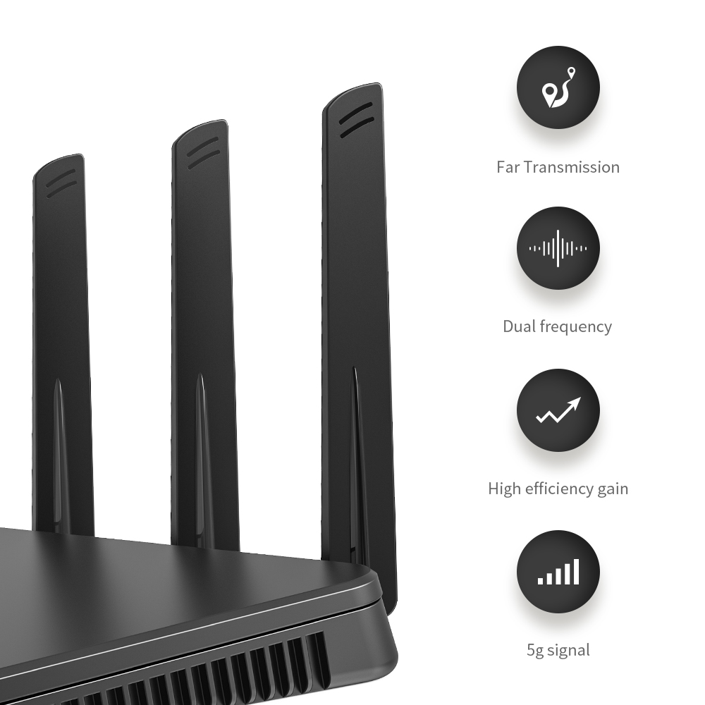
- The Picture of wifi Antenna
-

Wifi Antenna,Wifi Antenna for PC,Wifi Antenna for Router,Wfi Antenna outdoor,Wifi Antenna Indoor
Yetnorson Antenna Co., Ltd. , https://www.xhlantenna.com