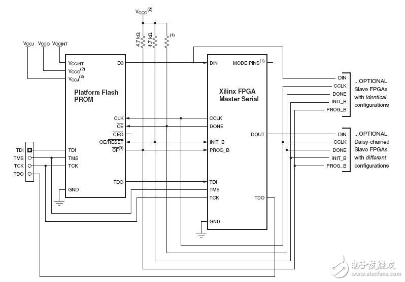
Here is the configuration circuit of Xilinx's spartan-3 series FPGA. Of course, other series of FPGA configuration circuits are similar, readers can analogy, with reference to the officially provided datasheet, after all, that is the most authoritative data.
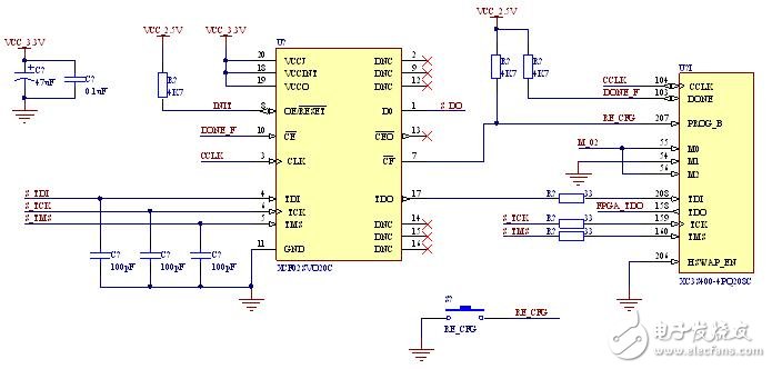
The so-called typical, here is to list the configuration circuit of the xc3s400, the most common spartan-3 on the market. All spartan-3 FPGA configuration circuits are linked in the same way. Xc3s400 is a 400,000-gate FPGA. Although its ConfiguraTIon Bitstream is only 1.699136Mbit, it still needs 2Mbit configuration chip XCF02S. I can't take it for granted that my design is simple and I use up to 1Mbit. Then I can choose XCF01S (1Mbit). . This is not the case. Even if you just use xc3s400 to design a street light, then the data you download to ROM (XCF02S) is 1.699136Mbit, so the choice of FPGA configuration ROM should be small.
There are five types of configuration circuits: main string, slave string, master sum, slave, and JTAG. The first four are relative to the download to the PROM (string is different from the different configuration chip is the serial port and the time parallel port protocol and FPGA communication), only JTAG is relative to debugging is to download the configuration to the FPGA RAM (lost after power down). Compared with CPLD, CPLD is based on ROM type, which is to download data to CPLD and not lose it after power failure. The FPGA is based on RAM. If there is no external ROM to store the configuration data, then the data will be lost after power failure. Therefore, FPGAs need to have external configuration chips (of course, there are also FLASH-based FPGAs). Then we will look at the connection of the FPGA configuration circuit in the main string mode.
The official hardware connections are as follows :

In order to increase the reliability of the configuration circuit, we usually add some anti-interference design (such as adding filter capacitors, matching resistors):

Look at the pins of the PROM chip first. 18,19,20 feet will not talk, according to the datasheet to provide the corresponding level; 3 feet CLK is connected to the FPGA CCLK, data communication synchronization is through the clock generated by the FPGA CCLK; because the chip used When the serial configuration chip, so only one data signal port DO, connected to the DIN port of the FPGA (not shown in the above figure), and the above clock signal work together to complete the serial data transmission, whenever the rising edge of CLK is latched Data, while the address counter inside the PROM is automatically incremented; there are two control signal lines, INIT (OE/RESET connected to the PROM) and DONE (CE connected to the PROM). OE/RESET is to ensure that the pre-PROM is reconfigured each time. The address counter is reset; regarding the CE pin, the official information is not very detailed. In my personal understanding, CE should be the abbreviation of chip enable. From the connection with the DONE pin of the FPGA, it is not difficult to infer that the FPGA is not configured. When DONE=0, then the configuration chip PROM is in the chip select state, and once the configuration completes DONE=1, the PROM is no longer strobed, and the datasheet also says that the pin can be directly grounded, that is, the slice is always Checked, but this will cause the DATA port to have continuous data signal output, and cause unnecessary current consumption; the CEO pin is not connected here because it is used as the OE end signal connection of the next PROM in the configuration circuit of multiple PROMs. The CF signal is connected to the FPAG's PROG_B interface. Its function is to generate the start configuration signal. It is connected to a pull-up resistor. If PROG_B generates a low-level pulse, the PROM will restart the configuration, so we will be in this section. Connect a button to the line on the line. If the button is pressed, the PROM will be enabled to reconfigure the FPGA. There are also several signal interfaces TDI, TCK, TMS, and TDO that are connected to the PROM and PC. The PC passes these circuits (usually After connecting a piece of drive isolation chip and communicating through the parallel port, we do not focus on the download data to the PROM.
When talking about the signal interface of the PROM, the configuration pins of the FPGA are mentioned. Here are some more inductive explanations. The FPGA has seven dedicated configuration pins (CCLK, DIN, PROG_B, DONE, HSWAP_EN, M0, M1, M2), four dedicated JTAG pins (TDI, TCK, TMS, TDO), these pins are made by VCCAUX Specially powered (this series of FPGAs are usually connected to VCCAUX = 2.5V). The M0, M1, and M2 pins of the FPGA are used for configuration mode selection. In the main string mode of the circuit, {M0, M1, M2} = 000, if the JTAG download mode {M0, M1, M2} = 101. The HSWAP_EN pin grounding not mentioned above is used to set the other idle pins to be pulled up when the FPAG is in the configuration state, and if the pin is connected to the high level, the FPAG is in the configured state and other idle pins. Floating. Therefore, in order to reduce the interference of the FPGA configuration process, this pin is generally grounded.
High Quality Solar Energy System Inverter For Selling
GuangZhou HanFong New Energy Technology Co. , Ltd. , https://www.zjgzinverter.com