Wafer cutting is a key part of the solar photovoltaic cell manufacturing process. This process is used to treat solid silicon ingots of monocrystalline or polycrystalline silicon. The wire saw first cuts the silicon ingot into cubes and then cuts it into very thin silicon wafers. (Fig. 1) These silicon wafers are substrates for manufacturing photovoltaic cells.
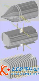
Figure 1. Three steps for wafer cutting: cut, cut and slice
Wafers are the most expensive part of crystalline silicon photovoltaic cell technology, so reducing the manufacturing cost of this part is critical to increasing the competitiveness of solar energy to traditional energy sources. This article will provide an overview of the silicon wafer slicing process, the challenges of manufacturing, and how the new generation of wire saw technology can reduce the cost of slicing.
History of wire saws
The first practical photovoltaic slicer was born in the 1980s and it stems from the cutting-edge research and work of Dr. Charles Hauser. Dr. Charles Hauser is the founder of the Swiss HCT slicing system and the predecessor of the PWS Precision Wafer Handling Systems Division of Applied Materials. These machines use a cutting line with a slurry to complete the cutting action. Today, the basic structure of the mainstream machine for silicon ingot and wafer cutting is still derived from Dr. Charles Hauser's original machine, but there has been a significant improvement in handling loads and cutting speeds.
Cutting process
The core of modern wire saws is an ultra-fine, high-strength cutting line that is used to complete the cutting action with the slurry. Up to 1000 cutting lines are wound parallel to each other to form a horizontal cutting line "net" on the wire wheel. The motor drives the wire wheel to move the entire cutting line at a speed of 5 to 25 meters per second. The speed, linear motion or back and forth motion of the cutting line is adjusted according to the shape of the ingot during the entire cutting process. During the movement of the cutting line, the nozzle continues to spray the slurry containing suspended silicon carbide particles to the cutting line.
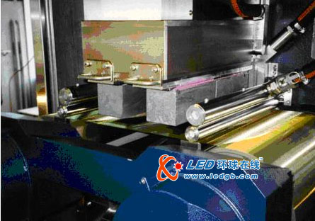
Figure 2. A cutting grid made up of silicon blocks through a cutting line.
The silicon block is fixed to the cutting table, usually 4 pieces at a time. The cutting table is cut by a moving cutting line to cut the silicon into silicon wafers (Fig. 2). The cutting principle seems to be very simple, but there are many challenges in the actual operation. The wire saw must accurately balance and control the wire diameter, cutting speed and total cutting area to achieve consistent wafer thickness and reduced cutting time without breaking the wafer.
Reduce silicon consumption
For silicon-based photovoltaic cells, crystalline silicon (c-Si) materials and cutting costs account for the largest portion of the total cost of the battery. Photovoltaic cell manufacturers can reduce costs by conserving silicon feedstock during the slicing process. This effect can be achieved by reducing the kerf loss, which is mainly related to the diameter of the cutting line and is the loss of raw materials produced by the cutting process itself. The diameter of the cutting line has been reduced from the original 180-160?m to the current commonly used 140-100?m. Lowering the diameter of the cutting line can also cut more silicon wafers under the same length of the silicon block to increase the output of the machine.
Making silicon wafers thinner also reduces silicon material consumption. In the past ten years, the thickness of photovoltaic wafers has been reduced from the original 330?m to the current 180-220?m range. This trend will continue, with wafer thicknesses of 100μm. The benefits of reduced wafer thickness are staggering, from 330μm to 130μm, photovoltaic cell manufacturers can reduce overall silicon feedstock consumption by up to 60%.