Abstract: According to the principle of VGA (Video Graphic Array) [1], an image display scheme based on Zedboard FPGA board is designed by using VHDL hardware description language. The experimental results show that the image display in the FPGA achieves the expected effect. According to this principle, the image acquisition and the display on the VGA display can be realized.
Introduction Using FPGA to generate VGA timing signals and transmitting image information as an image signal acquisition system will greatly reduce the difficulty and investment of image development [2]. There are many standards for the display of the display, such as VGA, SVGA, etc. In this design, a VGA image display controller based on Xilinx 7 series FPGA was designed and tested on the Zedboard board, and the penguin's head was successfully displayed on the display. By using this principle, the function of image display can be realized from the PC, and the cost investment can be reduced.
Principle of VGA
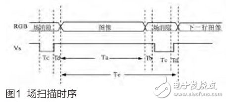
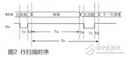
VGA has been widely used as a standard display interface. A common color display is generally composed of a CRT (cathode ray tube), and the color is composed of three colors of R, G, B (red: Red, green: Green, blue: B1ue). The display is a progressive scan method in which an electron beam emitted from a cathode ray gun is struck on a phosphor-coated phosphor screen to produce RGB three primary colors, and finally a color image is synthesized [3]. In the VGA interface protocol, different display modes have different timings or different refresh frequencies, so the timing is also different [4]. For each display mode timing, VGA has strict industry standards. Figure 1 and Figure 2 are timing charts of VGA line scanning and field scanning.


The picture display principle first uses Image2lcd software to convert the images we need into binary files. It should be noted that for different VGA interface design methods, the file format to be converted is also different. Here, the setting generates 256 colors. Image file.
The picture shows that the information of the picture needs to be sent to the VGA interface. The design adopts the scheme that when the pixel is counted and the field is counted, the picture information is directly assigned to the color signal R, G, B, and the display pixel of the picture is needed. Determine the corresponding position one by one.
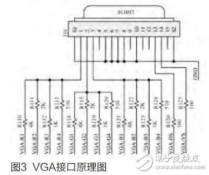
The implementation of the FPGA system here we use the Zedboard board as the control core, the schematic diagram of the VGA interface of the board is shown in Figure 3.

Timing signal
Zedboard provides a 50MHz clock signal, and the VGA display requires a 25.175 MHz clock. Therefore, the clock signal must be divided by two to get a 25 MHz clock frequency. We use the divided signal as the timing signal for HS and VS. Its VHDL program is designed as follows:
Process(clk_25M) -- Generates a field scan and line scan signal under the crossover signal implemented here
Begin
If clk_25M'event and clk_25M='1'
Then
If(hclk=800) then hclk<=0;
Else hclk<=hclk+1;
End if;
If hclk>=656 and hclk<752 then
Hs1<='0';
Else hs1<='1';
End if;
End if;
End process;
Process(hs1)
Variable cnt :integer range 0 to 1000
:=0;
Begin
If hs1'event and hs1='0' then
If vclk=524 then vclk<=0;
Else vclk<=vclk+1;
End if;
If vclk >= 491 and vclk<492 then
Vs1<='0';
Else vs1<='1';
End if;
End if;
End process;
The image display first needs to define an array of registers to store the image.
Type data_buffer is array(0to 22499) of std_logic_vector(7downto 0);
Constant buf:data_buer:=(⋯⋯--Define a 150&TImes;150 picture information here);
The output control of the image is performed on the basis of the generated field and line scan signals, and the display position is within a rectangle of a rectangle (100, 100, 250, 250). The control program is as follows.
Process(clk,vclk,hclk)
Begin
If clk'event and clk='1' then—control signals are output in a rectangle
If( vclk>=100 and vclk<250 and
Hclk>=100 and hclk<250) then
Dat 1 < = buf ( ( vclk -
100) *150+(hclk-100));
Else dat1<="00000000";
End if;
End if;
Image output uses Zedboard's VGA interface for data and timing signal output.
Hs<=hs1;
Vs<=vs1;--row, field signal output
Dat<=data1;--data output

Conclusion Using the FPGA to control the VGA for image output overcomes the drawbacks of having to use a PC as a control in the past, reducing the cost of investment. According to the principle of the design, the IP core of the FIFO of the FPGA can be used as the storage unit of the data to realize the display of the dynamic image, which is of great significance for realizing a small control system.
Bitcoin mining machines are one way to obtain bitcoins. Bitcoin is an online virtual currency created by open-source peer-to-peer software. Instead of being issued by a specific currency institution, and produced by the massive computation of a specific algorithm, the Bitcoin economy uses a distributed database of nodes throughout the P2P network to identify and record all transactions. The decentralized nature and algorithm of P2P can ensure that it is impossible to artificially manipulate the value of bitcoin by producing a large number of coins.
Any computer can become a mining machine, but the returns will be low, and it may not mine a single bitcoin in a decade. Many companies have developed specialized Bitcoin mining machines with special mining chips that are tens or hundreds of times faster than normal computers.
Currency system by the user (the user through the key control wallet), trade (trade will be broadcast to the whole currency network) and miners (generated by competition calculation agreed on each node of the chain block, block chain is a distributed public authority books, contains the currency network of all the transactions happened)
Bitcoin miners manage the Bitcoin network by solving the problem of proof-of-work mechanisms with a certain amount of work -- confirming transactions and preventing double payments. Because hashing is irreversible, finding the number of random adjustments required to match is difficult, requiring a trial-and-error process that can predict the total number of times. This is where the proof-of-work mechanism comes into play. When a node finds a solution that matches the requirement, it can broadcast its result to the whole network. Other nodes can then receive the newly solved data block and check whether it matches the rule. If the other nodes calculate the hash value and find that the requirement (the operation goal required by Bitcoin) is satisfied, then the data block is valid and the other nodes accept the data block.
Bitcoin Mining Machine:S19 Pro Hyd Asic Miner,S19 Pro Hyd Antminer Bitmain,S19 Hyd Bitmain Antminer,s19j pro antminer bitmain,whatsminer m50s,etc.
Bitcoin Mining Machine,Antminer S19j Pro,bitcoin Miner,btc mining machine,S19 Pro Hyd
Shenzhen YLHM Technology Co., Ltd. , https://www.sggminer.com