With the rapid development of China's Welfare Lottery business, the computer lottery sales system puts forward higher requirements for the control of betting machine operation and the collection of telemetry data. As the premise of real-time control and monitoring of Fucai sales system, data collection has no doubt played an important role. However, in the process of data acquisition, due to the interference factors such as harmonics, how to accurately and quickly collect the analog quantity of each module in the betting machine has been a hot spot in the sales system research.
In recent years, the performance of various integrated DSPs has been greatly improved, and prices have fallen sharply. More and more users have begun to use DSP devices to improve product performance. This paper designs a set of signal acquisition circuit based on ADS8365 and TMS320F2812. Its interface circuit is simple, the acquisition precision is high, and the speed is fast, which is the expected target.
1. Introduction to TMS320F2812TI (Texas Instruments) mainly promotes high-performance TMS320C28x series TMS320F2812 32-bit fixed-point micro-control unit (MCU) with frequency up to 150MHz; with I2C, SPI, CAN, PWM and other bus interfaces, suitable for various control industrial equipment; High performance, high portability, and suitable for a variety of handheld devices; Meet high and low temperature, vibration testing, to meet industrial environmental applications.
2.ADS8365 IntroductionThe ADS8365 is a high speed, low power, 6 channel simultaneous sampling and conversion, single +5V powered analog to digital conversion chip. Converts a maximum sampling throughput of up to 5MHz with a full-interpolation input channel with 80dB common-mode rejection and six differential sample-and-hold amplifiers. The pin also has a 2.5V reference and a high speed parallel interface.
3. Interface circuit design of ADS8365 and TMS320F2812Because the ADS8365 and TMS320F2812 are high-speed chips provided by TI, the two can be perfectly matched in speed to achieve seamless connection between chips.
PTout is an analog signal input with a voltage range of -5V to +5V and is input to the analog input channel A0 of the ADS8365 via a differential circuit. The interface selects the 16-bit data output mode, so the BYTE and ADD pins of the ADS8365 are grounded. The reading of the conversion result for each channel is selected by address lines A2, A1, A0. The chip select signal of ADS8365 is generated by F2812 address line A15, A14, A13 and I/O space chip select line XZCS# through 74LV138. ADS8365 chip address occupies the low 32K address space of F2812I/O space, and program. The debug is independent of the running address.
In order to achieve simultaneous sampling of the six channels of the ADS8365, the ADS8365 A, B, C three group start control signals HOLDA#, HOLDB# and HOLDC# are controlled by the same I/O pin of F2812, so as long as F2812 makes this pin valid. Six channels of the ADS8365 can be simultaneously activated to achieve simultaneous sampling of six channels.
The clock signal of the ADS8365 is provided by the output signal T4PWM of Timer 4 of F2812 with a frequency of 3.75MHz. The A/D chip is also reset when the DSP is reset. The A/D conversion end signal is connected to the external interrupt pin XINT2 of the DSP. Therefore, the A/D conversion result can be read by interrupt and query, depending on the specific requirements of programming and engineering applications.
The ADS8365 is powered by a +5V analog supply (AVDD) and a +5V digital supply (DVDD), while its internal buffer uses the same +3.3V voltage as the F2812. The buffer voltage (BVDD) allows direct connection to a 3V or 5V voltage system. The I/O voltage of the F2812 is +3.3V. Therefore, if this component is used, the BVDD of the ADS8365 must be set to 3.3V.
4. TMS320F2812 settings(1) Conversion clock setting In this system, PWM signal of F2812 is used to provide clock signal for ADS8365, PWM2 is set to work in full comparison mode, and output is active high. Set the F2812 system clock SYSCLKOUT=90MHZ, then the high-speed peripheral clock HSPCLK=SYSCLKOUT/2=45MHz. Set the period register value of general-purpose timer T1 to 12 (T1PR=0x000c), and the value of the compare register to 6 (T1CMPR=0x0006). Therefore, the output clock frequency is CLK=HSPCLK/T1PR=3.75MHz, which is in accordance with the maximum clock frequency of ADS8365. For 5MHz requirements.
(2) Output port setting PWM1/GPIOA0, PWM3/GPIOA2 are GPIO outputs, GPIOA0 is used to control the RESET# signal of ADS8365, and GPIOA2 controls HOLDA#, HOLDB# and HOLDC# signals. Port E's XINT2_ADCSOC is set to the interrupt input signal
At the end of ADS8365 data conversion, the pin EOC# goes low, triggers the XINT2# interrupt, enters the interrupt service routine, and performs data read operation. When the chip select (CS#) of the ADS8365 is high, the parallel data output pin D[15:0] is in a high impedance state. When it is low, the parallel data line reflects the current state of the output buffer. In order to properly read data from the parallel bus of the ADS8365, it must be set low. Since the XZCS2# of the F2812 is selected as the chip select signal of the ADS8365, the ADS8365 address is mapped to the extended bus memory space XINTF Zone2 of the F2812. Use the A9, A5, and A3 output pins of the F2812 to control the A0-A2 data address of the ADS8365, as shown in Table 1.

The read pointer is pointed to the first reading position by triggering the reset pin of the ADS8365 low. The pin REST# of the ADS8365 is controlled by GPIOA0. As part of the F2812 initialization, GPIOA0 is initially high and is asserted low when the system clock is stable, ensuring that the data output from the ADC follows the order of channels A0, A1, B0, B1, C0, C1.
Data Acquisition HOLDX# is an active low level sampling trigger. The conversion begins when the HOLDX# of the ADS8365 remains low for at least 20ns. By connecting all three HOLD signals to GPIOA2, the sample-and-hold amplifiers of each channel are held at the same time, allowing each channel to start conversion at the same time.
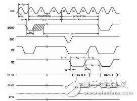
When the conversion result is stored in the output register, the pin EOC# will remain low for half a clock cycle. In addition, by setting RD# and CS# to a low level, data can be read out to the parallel output bus. Read (RD#) and write (WR#) are active low level input signals. When CS# is low, the output buffer of the ADS8365 is updated on the falling edge of RD#. This means that the RD# signal must be triggered once before each read sequence, so that the newly acquired data can be read. Its read timing diagram is shown in Figure 2.

Figure 2 reads the ADS8365 timing diagram
6. Software designIn order to facilitate debugging and maintenance, the software design follows a modular, top-down, and gradually refined programming philosophy. The software is a mixture of C and assembly language programming. After the system power-on reset, first boot the loader according to the selected mode, jump to the main program entry, and then initialize the relevant variables, data buffers, control registers, and status registers. After resetting and initializing the external ADS8365, waiting for the external interrupt, the A/D converted data is read into the allocated data buffer in the interrupt service subroutine, and the F2812 is the fixed point DSP. In order to improve the accuracy and speed of the operation, software design Make full use of the IQmath Library provided by TI to realize the seamless interface between floating-point arithmetic and fixed-point program code, simplify the development of the program, and greatly improve the real-time performance of the program. The main code is as follows (take CHA0 as an example):
Void main(void)
{
ptrCHA0=(int*)CHA0; InitSysCtrl();
InitGpio();
ResetADS8365();
DINT;
PieCtrlRegs.PIEIER1.bit.INTx5=1;
XIntruptRegs.XINT2CR.all=0x0000;read_A();
XIntruptRegs.XINT2CR.all=0x0001;
PieCtrlReg.PIEACK.all=0x0001;return;
}
Information technology has penetrated into all areas of our lives. With the progress of technology, the iteration rate of laptops is getting faster and faster. Previous laptops mainly used E-SATA, FireWire, VGA, DisplayPort, SD card slot, USB A, 3.5mm headphone jack, HDMI or RJ45 ports.But manufacturers began stripping connectors from laptops to make them thinner and lighter. Most new laptops now have a USBC port (Thunderbolt or full-featured USBC) and an audio jack. The laptop is thin, but the missing ports are useless. This is where the USB C Hubs comes in.
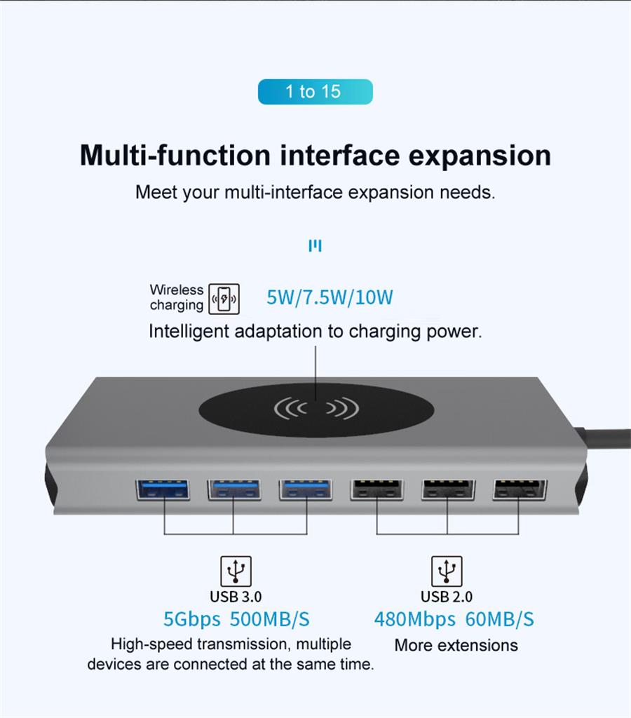
Type C Usb Hub can support USB, PD, DisplayPort, Thunderbolt, and other protocols. Using USB HUBS, you can extend multiple common connectors directly to your laptop. Mosses are compact, so you can take them anywhere. All peripheral devices are centrally connected to the hub, which reduces the hassle of plugging in and out of the laptop port and makes your desktop cleaner. Let's take a closer look at its capabilities so you can determine how many ports you need.
So these are all important ports on the hub, with the exception of the 3.5mm audio jack. Also, while aesthetics are not important, choosing a nice hub will make you happier. There are rectangular, square, and circular centers on the market to meet your desk setup needs. Usually, the rectangular type is best for your desk because the cables can be well organized if all the ports are on one side of the center.

Usb C Hubs,4 Port Usb C Hub,Usb C Multiport Hub,Usb Hub With Hdmi Port
Henan Yijiao Trading Co., Ltd , https://www.yjusbhubs.com