Pure semiconductors are doped with trace amounts of impurity elements, and the resulting semiconductors are called impurity semiconductors. Semiconductors can be classified into P-type semiconductors and N-type semiconductors depending on the type of impurity element incorporated. Diodes have PN junctions, using different doping processes, through the role of diffusion, the P-type semiconductors and N-type semiconductors are fabricated on the same semiconductor substrate, forming a space charge region at their junction called a PN junction, PN junction has Unidirectional conductivity.
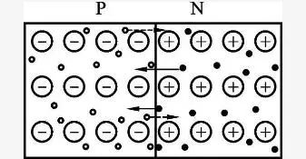
PN Junction Formation When P-type semiconductors and N-type semiconductors are fabricated together, at their interfaces, because the concentration of majority carriers in the two semiconductors is very different, holes in the P region will diffuse toward the N region. At the same time, free electrons in the N area will also spread to the P area, as shown in Figure 1. Arrows in the figure indicate the moving direction of holes in the P region, and solid arrows indicate the moving direction of the free electrons in the N region.


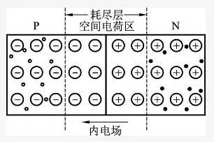
Free electrons that diffuse into the P region encounter holes that recombine, and holes and free electrons that diffuse into the N region also recombine, so the concentration of multiple sons at the interface decreases, and the negative ion region appears in the P region, and the N region appears positive. The ion region is called the space charge region. After the space charge region appears, an electric field is formed in the space charge region due to the interaction between positive and negative charges. The direction of the electric field is directed from the positively charged N region to the negatively charged P region. Since this electric field is formed by carrier diffusion motion (ie, internal motion) rather than applied voltage, it is called an internal electric field. As the diffusion motion progresses, the space charge region widens and the internal electric field increases. The direction just blocks the multi-sub-hole free electrons in the P region and the multiple free electrons in the N region.
Under the action of internal electric field electric field force, the minority son free electrons in the P region will drift to the N region, and the minority son holes in the N region will also drift to the P region. The direction of drift motion is exactly opposite to the direction of diffusion motion. The holes drifting from the N region to the P region complement the holes lost in the P region of the original interface, and the free electrons drifting from the P region to the N region complement the free electrons lost in the N region of the original interface. Makes space charge less. It can be seen that the effect of drifting motion is to narrow the space charge zone, which is the opposite of the effect of diffusion motion. In the absence of external electric field and other excitations, when the number of multiple sons involved in diffusion motion is equal to the number of minority sons involved in drift motion, it reaches a dynamic equilibrium. This is a certain thickness of space charge area formed on both sides of the interface, called the PN junction. . This space charge region hinders the diffusion of many sons, so it is also called a barrier layer; and because there is almost no carrier, it is also called a depletion layer. The PN junction is shown in Figure 2.

Diesel Pressure Sensor,Hydraulic Pressure Gauge,Rail Pressure Sensor,Absolute Pressure Transmitter
Shenzhen Ever-smart Sensor Technology Co., LTD , https://www.fluhandy.com