At present, video surveillance is widely used in security monitoring, industrial monitoring and traffic monitoring. The video surveillance system generally goes through three stages: firstly, the TV monitoring system based on analog signal, its function is single, susceptible to interference and difficult to expand; then the PC-based image monitoring system appears, and its terminal function is strong. However, the price is expensive and the stability is poor. In recent years, with the maturity of embedded technology, the embedded video acquisition and processing system has the advantages of high reliability, high speed, low cost, small size, low power consumption and strong environmental adaptability.
Video signal processing circuit
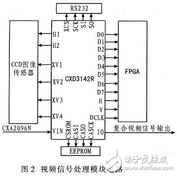
This design uses SONY's dedicated signal processing device CXD3142R as the signal processor. The CXD3142R is a low-power, high-efficiency signal processor designed to process Ye, Cv, Mg, and G complementary color single-chip CCD output signals. It has automatic exposure and auto white balance to simultaneously output composite video signals and YUV 8 Bit digital signal output. The internal 9-bit A/D converter synchronization signal generation circuit, external synchronization circuit and clock control circuit are integrated. In addition, the CXD3142R also has a serial communication function. The user can preset the register value in the DSP in the PC, download it to the DSP through the serial port, and perform automatic exposure and automatic white balance processing on the image signal. 2 is a circuit connection diagram of a video signal processing module.

In Fig. 2, H1, H2, XV1, XV2, XV3, and XV4 are timing driving signals of the CCD image sensor, and the EEPROM is used to store the register value initialized by the DSP. D0~D7 are YUV digital signals. The specific workflow: after the analog signal collected by the CCD image sensor is pre-processed by CXA2096N, the corresponding digital signal is transmitted to the DSP (CXD3142) via the VIN pin. After receiving the digital signal, the DSP uses its internal AE/AWB detection circuit. The synchronization signal generation circuit, the external synchronization circuit and the related algorithm perform related processing on the same, and after the processing is completed, the 8-bit digital signal is passed under the control of the line (H pin), the field (V pin) signal and the clock signal (PCLK). The D0~D7 pins are passed to the FPGA module for processing. Through the SCK, SI, SO, XCS serial communication, the CSROM, CASI, CSASO, and CASCK ​​pins communicate with the external EEPROM to implement DSP-related initialization. In addition, the IO pin outputs the composite video signal processed by the DSP, and the image processing result is directly displayed on the CRT display through the relevant interface.
Peripheral interface module
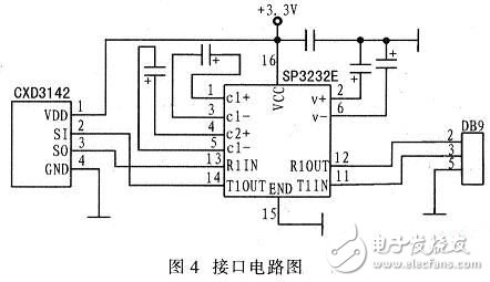
This design supports RS-232C serial communication. However, the serial communication needs to convert the 3.3 V logic level to the RS-232C standard level. Therefore, level conversion is performed using SP3232E series devices. The SP3232E generates an RS-232C voltage level of 2Vce from a supply voltage of +3.0 to +5.5 V. This series is suitable for +3.3 V systems. The SP3232E device has a typical data rate of 235 kb/s at full load. Figure 4 is an interface circuit diagram of the system design.

It should be noted that due to the limited driving capability of the SP3232E device, the interface circuit is only suitable for short-distance transmission. If long-distance transmission is required, the signal transmission capability must be enhanced.
men's quartz field watch,stainless steel men's quartz watch,quartz movement watch,quartz watch water resistant
Dongguan Yingxin Technology Co., Ltd. , https://www.yingxinkeyboard.com