"LED flip-chip technology +, there are three main aspects +. First, LED flip + material; second, LED flip + process and equipment; third, LED flip + product." Manager Qian Xuexing said at the 15th High-tech LED Industry Summit Forum on June 10.

Qian Xuexing, General Manager of Morning Technology
It is understood that LED flip-chip + materials mainly include chips, phosphors, brackets, solid crystal solder paste, packaged silica gel, etc.; LED flip-chip + process and equipment mainly include CSP process and equipment, integrated technology and equipment; LED flip-chip + The products mainly include bulb COB, flexible filament, car lamp, small pitch RGB, strip lamp, etc. It can be judged that the flip-chip package will cover most of the existing lighting, display, car lights and other applications in the future.
The integrated packaging process is the invention patent that was independently researched and developed in the morning in 2013. It is also the first company to define the LED flip-chip packaging process. The integrated package is to directly bond the chip to the substrate through the die-bonding solder paste. The optical parameter of the fruit powder glue is spotted on the substrate to form a point source and a strip light source.
Fruit powder glue is also called high-touch-type glue. The phosphors are mixed with silica gel to a corresponding standard light color parameter according to a certain ratio, and the phosphor powder system is used to maintain the phosphor powder without precipitation during the shelf life. Fruit powder glue and CSP fluorescent glue have similarities, but their respective methods of use are quite different from those of equipment. In the past two years, the company has been leading the development of fruit powder glue and formed its own intellectual property rights. It is expected to simplify the flip-chip process through material changes.
In the process, the powder of the LED integrated packaging process is applied to the flip chip by a dispensing device under specific pressure parameters, and is heated and solidified into a finished product. The CSP process is to cure the phosphor-containing film to the five sides of the flip chip non-electrode or to form a single-sided heat curing, and then cut the sealed flip chip into a miniaturized electronic light-emitting device by cutting. The braiding method is packaged for easy patching.
According to Qian Xuexing, “the LED integration process is simple, the production equipment is small, the circuit board is packaged, and there are no additional processes such as patching. However, the disadvantage is that it cannot be split, and the consistency of the powder coating control and optical parameters is high; The CSP packaging process can realize miniaturization and ultra-thinness of the light-emitting device, but the disadvantage is that the process is complicated, the equipment is large, and the cutting precision is high."
It is well known that flip-chips not only play the role of conduction, heat conduction, reflection, protection and load-bearing in the flip-chip package, but their solid crystal function position is the eutectic reaction material of flip-chip soldering, so the choice of pad material is for the solid crystal solder paste. The welding effect has a certain influence.
“In fact, 2016 is the fastest development of COB. From COB aluminum substrate to ceramic substrate to flexible filament to SMD bracket behind, the original SMD is not suitable for flip-chip. Later, we are working with several big manufacturers. In the process, I made some upgrades to the plating and structure," Qian Xuexing said.
In addition, the solid crystal solder paste is the key to the flip-chip innovation, not only the decisive material for conducting and conducting heat, but also the key factor for wafer bonding, which makes the LED bonding jump from the physical bonding of the glue to the chemical combination of the solder paste alloy. Price combination. The quality of the flip-chip product is inseparable from the solid crystal solder paste.
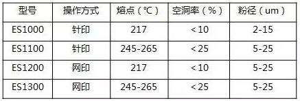
The corresponding parameters of each type of solid crystal solder paste

The manufacturing process of LED package + encapsulant has certain influence on the encapsulation. The traditional encapsulation process is that the phosphor and A/B glue are mixed and stirred in a certain proportion, and the glue is removed after defoaming. In the LED integrated packaging process, the fruit powder glue does not need the packaging engineer to match the phosphor and adjust the optical parameters.
It can be seen that different packaging adhesives make the LED manufacturing process simple. The CSP packaging process is mainly embodied in miniaturization and standardization of the light source device. The SMD light source device of our current package is first sealed and then applied. The fruit powder glue helps the integrated package directly in the application end glue, and the process equipment is simpler.
For the LED integrated manufacturing process, there are five main steps:
A, select the appropriate LED flip-chip light-emitting chip, and install the LED chip directly on the flip-chip eutectic layer on the PCB circuit board;
B. Perform reflow eutectic soldering on the PCB circuit board of the mounted LED flip-chip light-emitting chip;
C, detecting the LED after eutectic;
D, performing residual cleaning on the tested eutectic LED;
E, silicone packaging of the PCB circuit board;
It is worth mentioning that the current technology has already achieved "a chip-packaged solid crystal solder paste and its preparation method and use process", "LED integrated manufacturing process", "a high-thixotropic LED with phosphor deposition "Powder Gum" and other LED flip-chip related invention patents, through the intellectual property and material solutions, to lay out the future LED flip-chip market.

Rechargeable Vape Pen,Rechargeable Battery Vape Pen,Rechargeable Disposable Vape Pen,Vape Pen For Smoke Oil
Shenzhen Essenvape Technology Co., Ltd. , https://www.essenvape.com