Designers must meet many of the electromagnetic compatibility (EMC) requirements for automotive applications, and choosing the right switching frequency (fsw) for the power supply is critical to meeting these requirements. Most designers choose the switching frequency outside the mid-wave AM broadcast band (typically 400 kHz or 2 MHz) where electromagnetic interference (EMI) must be limited. The 2MHz option is ideal. Therefore, in this blog post, I will provide some key considerations when trying to operate with TI's new TPS54116-Q1 DDR memory power solution as an example at 2MHz.
The first and most important consideration when operating at 2MHz switching frequency is the minimum turn-on time of the converter. In a buck converter, when the high-side MOSFET is turned on, it must maintain a minimum on-time before shutting down. With peak current mode control, the minimum on-time is typically limited by the blanking time of the current sense signal. The maximum minimum on-time of the converter typically occurs under minimum load conditions for three reasons.
Under heavy load conditions, there is a DC drop in the circuit, which increases the work-on time.
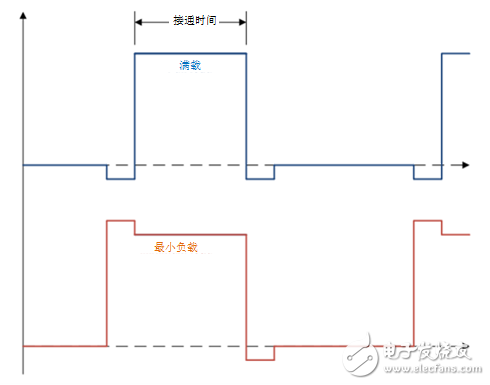
The rise and fall times of the switch node. During dead time (from the time when the low-side MOSFET is turned off to the high-side MOSFET turn-on, and the time between the high-side MOSFET turn-off and the low-side MOSFET turn-on), the current through the inductor is at any parasitic capacitance at the switch node. Charge and discharge. Under light load conditions, the current in the inductor is less, so the charge and discharge speed of the capacitor is slower, resulting in longer rise and fall times at the switch node. Longer rise and fall times result in an increase in the effective pulse width at the switch node.
Low to high dead time. The current through the inductor charges the voltage at the switch node until the low-side MOSFET turns off and the high-side MOSFET turns on again until the body diode of the high-side MOSFET clamps the switch node voltage. As a result, the switch node is high during the low-side MOSFET of the dead time when it is turned off to the high-side MOSFET. Since the switching node is high during this time period, the low to high dead time increases the effective minimum pulse width. In Figure 1, you can see that although the on-time is the same, the pulse width is larger.

Figure 1: Pulse width at full load and no load
The second consideration when attempting to operate at 2MHz is the conversion ratio of the minimum input voltage (VIN) to the output voltage (VOUT). This is related to the minimum on-time of the converter because this ratio sets the on-time when the converter needs to operate. For example, if the converter has a minimum on-time of 100 ns and operates at 2 MHz, Equation 1 is used, which can support a minimum conversion ratio (Dmin) of 20%. If the given VIN to VOUT ratio is less than the minimum on-time required, most converters enter pulse-crossing mode to keep the output voltage stable. When the pulse crosses, the switching frequency changes and may cause noise in the frequency where noise is required to be limited.
In automotive applications where the power supply is connected to the battery, the on-time must support a typical VIN range conversion from 6V to 18V. Using Equation 2 (18V maximum input and 20% conversion ratio), the minimum output voltage is 3.6V. When directly connected to the battery, large voltage spikes beyond this typical range may occur (eg, during load dump). Depending on the requirements of the application, the converter may be allowed or not allowed to pulse across during input voltage spikes.
A regulator connected to a 3.3V or 5V rail can work more easily at 2MHz. For example, the TPS54116-Q11 has a maximum on-time of 125ns, so at 2MHz, the minimum duty cycle is 25%. The minimum output voltage supported by the 3.3V input is 0.825V; the minimum output voltage supported by the 5V rail is 1.25V. A comprehensive analysis of the minimum output voltage for a given application should also include tolerances for VIN and switching frequency.
A third consideration when trying to operate at 2MHz is the AC loss in the inductor. The AC loss increases as the switching frequency increases, so it is important to consider when choosing a 2MHz inductor. Some inductors use core materials with lower AC losses to provide better efficiency at higher frequencies. Most inductor suppliers offer a tool to evaluate the AC losses in their inductors.
The fourth consideration when trying to operate at 2MHz is the trade-off between size and efficiency. When choosing a switching frequency for a DC/DC converter, a trade-off must be made between size and efficiency. The inductor size and some converter losses increase as the switching frequency increases. Specifically, when compared to the 400 kHz and 2 MHz conditions, the 2 MHz design will use 5 times smaller inductors, but with 5 times greater switching losses. A 5x smaller inductor means a smaller inductor size.
The two main losses in the converter frequency dependent converter are the switching losses of the high side MOSFET and dead time loss. Equation 3 is a basic estimate of these losses, and you can use it to further analyze the effects associated with higher switching frequency loss increases. For example, for a 5V input, 4A load, 3ns rise time, 2ns fall time, 0.7V body diode drop, and 20ns dead time, the estimated power loss is 325mW at 2MHz and 65mW at 400kHz.
Car Charger,Car Phone Charger,Car Mobile Charger,Wireless Car Charger
SUNSHINE ELECTRONICS TECH. CO., LTD. , https://www.benefitucx.com