AMBA
AMBA (Advanced Microprocessor Bus Architecture) is an open SoC bus standard proposed by ARM, which has been widely used in the core of RISC.
AMBA defines a multi-bus system (mulTIlevel busing system), including system bus and peripheral bus with lower level.
AMBA supports 32-bit, 64-bit, 128-bit data buses, and 32-bit address buses, and supports byte and half-word designs.
It defines two types of buses: AHB (Advanced High-performance Bus) Advanced high-performance bus, also known as ASB (Advanced System Bus). APB (Advanced peripheral Bus)
AHB and ASB are actually a thing, a high-speed bus, mainly responsible for the interface of embedded processor, DMA controller, Memory and so on.
APB is a low-speed bus, mainly responsible for peripheral interfaces
The bridge between AHB and APB is through Bridge
Bus Bridges
It is well known that the communication between the various modules in a system is through the bus. The function of the bus is to carry data and addresses from device A to device B.
If device A and device B have consistency (the original text is under discussion, I do n’t know how to translate better here, but for the time being translated to consistency), then device A and device B can be directly hung on the same bus and directly interpreted Data on the bus.
However, if device A and device B do not have consistency, then device A and device B must be hung on two different buses, at this time we need a "translation", the data on the bus on device A and The address is converted into a format that Device B can parse, and then put on the bus of Device B. This "translation" is "Bus Bridge",
The following picture illustrates the role of Bus Bridge between AHB and APB.
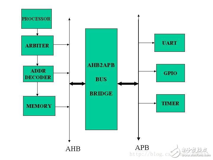
The data transmission speed of the AHB-linked device is much faster than the transmission speed of the APB device, that is, the role of the Bus Beidge here is to "buffer"
Here you can see that AHB is mainly linked to the kernel and storage management of the system, and APB is mainly distributed to my peripherals.
The following picture, it is easier to see the role of AHB and APB: AHB is linked to the system bus, RAM, etc. APB is linked to commonly used peripherals: GPIO, UART, etc.
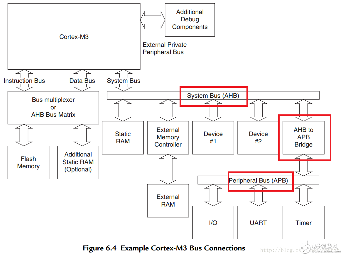
Bus structure on STM32
First look at the bus structure of the F103 series of chips
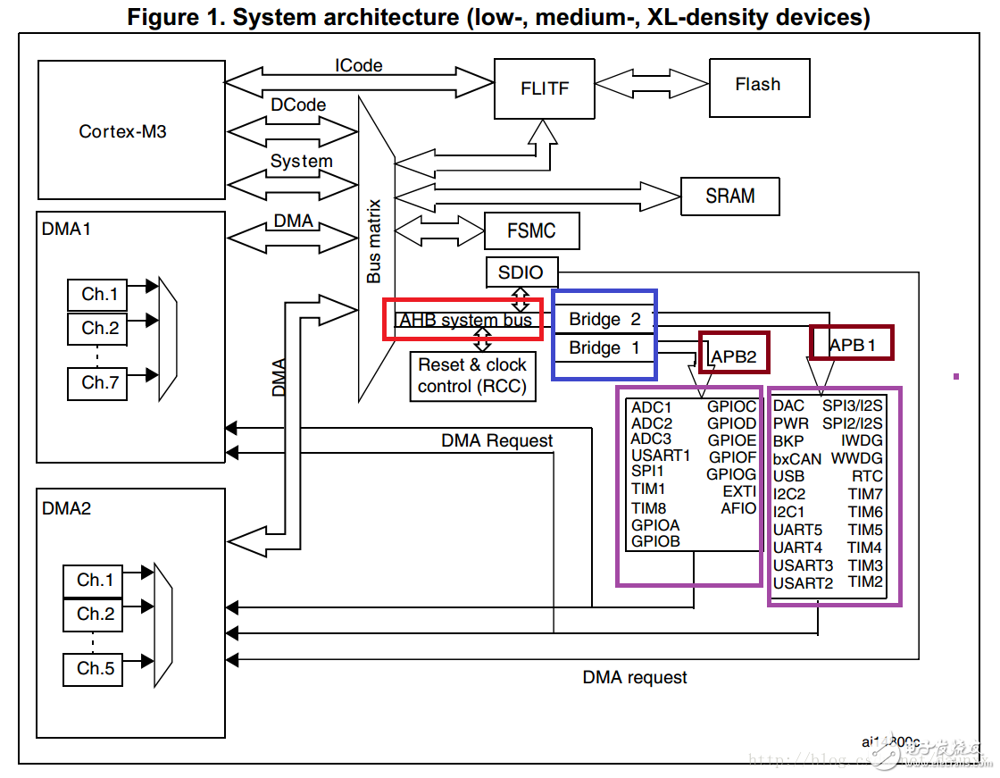
It should be noted that there are two APBs, and the peripherals they link are different, so there will be definitions of APB1 and APB2 in the STM32 library file:
/ ** @defgroup APB2_peripheral
* @ {
* /
#define RCC_APB2Periph_AFIO ((uint32_t) 0x00000001)
#define RCC_APB2Periph_GPIOA ((uint32_t) 0x00000004)
#define RCC_APB2Periph_GPIOB ((uint32_t) 0x00000008)
#define RCC_APB2Periph_GPIOC ((uint32_t) 0x00000010)
#define RCC_APB2Periph_GPIOD ((uint32_t) 0x00000020)
#define RCC_APB2Periph_GPIOE ((uint32_t) 0x00000040)
#define RCC_APB2Periph_GPIOF ((uint32_t) 0x00000080)
#define RCC_APB2Periph_GPIOG ((uint32_t) 0x00000100)
#define RCC_APB2Periph_ADC1 ((uint32_t) 0x00000200)
#define RCC_APB2Periph_ADC2 ((uint32_t) 0x00000400)
#define RCC_APB2Periph_TIM1 ((uint32_t) 0x00000800)
#define RCC_APB2Periph_SPI1 ((uint32_t) 0x00001000)
#define RCC_APB2Periph_TIM8 ((uint32_t) 0x00002000)
#define RCC_APB2Periph_USART1 ((uint32_t) 0x00004000)
#define RCC_APB2Periph_ADC3 ((uint32_t) 0x00008000)
#define RCC_APB2Periph_TIM15 ((uint32_t) 0x00010000)
#define RCC_APB2Periph_TIM16 ((uint32_t) 0x00020000)
#define RCC_APB2Periph_TIM17 ((uint32_t) 0x00040000)
#define RCC_APB2Periph_TIM9 ((uint32_t) 0x00080000)
#define RCC_APB2Periph_TIM10 ((uint32_t) 0x00100000)
#define RCC_APB2Periph_TIM11 ((uint32_t) 0x00200000)
#define IS_RCC_APB2_PERIPH (PERIPH) ((((PERIPH) & 0xFFC00002) == 0x00) && ((PERIPH)! = 0x00))
/ **
* @}
* /
/ ** @defgroup APB1_peripheral
* @ {
* /
#define RCC_APB1Periph_TIM2 ((uint32_t) 0x00000001)
#define RCC_APB1Periph_TIM3 ((uint32_t) 0x00000002)
#define RCC_APB1Periph_TIM4 ((uint32_t) 0x00000004)
#define RCC_APB1Periph_TIM5 ((uint32_t) 0x00000008)
#define RCC_APB1Periph_TIM6 ((uint32_t) 0x00000010)
#define RCC_APB1Periph_TIM7 ((uint32_t) 0x00000020)
#define RCC_APB1Periph_TIM12 ((uint32_t) 0x00000040)
#define RCC_APB1Periph_TIM13 ((uint32_t) 0x00000080)
#define RCC_APB1Periph_TIM14 ((uint32_t) 0x00000100)
#define RCC_APB1Periph_WWDG ((uint32_t) 0x00000800)
#define RCC_APB1Periph_SPI2 ((uint32_t) 0x00004000)
#define RCC_APB1Periph_SPI3 ((uint32_t) 0x00008000)
#define RCC_APB1Periph_USART2 ((uint32_t) 0x00020000)
#define RCC_APB1Periph_USART3 ((uint32_t) 0x00040000)
#define RCC_APB1Periph_UART4 ((uint32_t) 0x00080000)
#define RCC_APB1Periph_UART5 ((uint32_t) 0x00100000)
#define RCC_APB1Periph_I2C1 ((uint32_t) 0x00200000)
#define RCC_APB1Periph_I2C2 ((uint32_t) 0x00400000)
#define RCC_APB1Periph_USB ((uint32_t) 0x00800000)
#define RCC_APB1Periph_CAN1 ((uint32_t) 0x02000000)
#define RCC_APB1Periph_CAN2 ((uint32_t) 0x04000000)
#define RCC_APB1Periph_BKP ((uint32_t) 0x08000000)
#define RCC_APB1Periph_PWR ((uint32_t) 0x10000000)
#define RCC_APB1Periph_DAC ((uint32_t) 0x20000000)
#define RCC_APB1Periph_CEC ((uint32_t) 0x40000000)
#define IS_RCC_APB1_PERIPH (PERIPH) ((((PERIPH) & 0x81013600) == 0x00) && ((PERIPH)! = 0x00))
/ **
* @}
* /
The rate of APB is described below:

APB1 is limited to 36MHz, APB2 can also reach full speed 72MHz
The following is the bus architecture of F105 and F107:
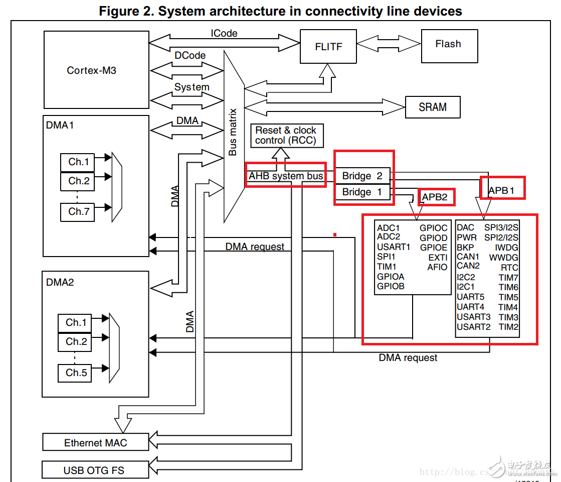
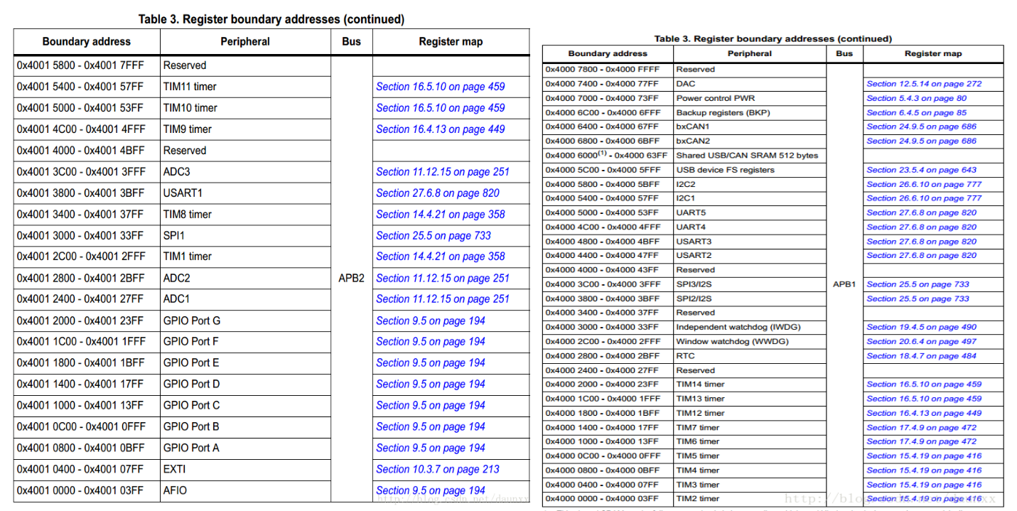
Address mapping of APB1 and APB2 on STM32
Innosilicon is a worldwide one-stop provider of high-speed mixed signal IPs and ASIC customization with leading market shares in Asian-Pacific market for 10 consecutive years. Its IP has enabled billions of SoC's to enter mass production, covering nodes from 180nm to 5nm across the world`s foundries including: GlobalFoundries, TSMC, Samsung, SMIC, UMC and others. Backed by its 14 years of technical expertise in developing cutting-edge IPs and ASIC products, Innosilicon has assisted our valued partners including AMD, Microchip and Microsoft to name but a few, in realizing their product goals.
Innosilicon team is fully devoted to providing the world's most advanced IP and ASIC technologies, and has achieved stellar results. In 2018, Innosilicon was the first in the world to reach mass production of the performance-leading GDDR6 interface in our cryptographic GPU product. In 2019, Innosilicon announced the availability of the HDMI v2.1 IP supporting 4K/8K displays as well as our 32Gbps SerDes PHY. In 2020, we launched the INNOLINK Chiplet which allows massive amounts of low-latency data to pass seamlessly between smaller chips as if they were all on the same bus. With a wide range of performance leading IP in multiple FinFET processes and 22nm planar processes all entering mass production, Innosilicon's remarkable innovation capabilities have been proven in fields such as: high-performance computing, high-bandwidth memory, encrypted computing, AI cloud computing, and low-power IoT.
Innosilicon Mining Machine:Innosilicon T2 Turbo 25T,Innosilicon T3+ 52T,Innosilicon T3 43T,Innosilicon T2 Terminator,Innosilicon T3 39T,Innosilicon T2 Turbo+ 32T
Innosilicon Mining Machine,T3 Pro Miner,T3 Pro Innosilicon,T3 Pro 67T Innosilicon
Shenzhen YLHM Technology Co., Ltd. , https://www.hkcryptominer.com