The problem that occurred on the ASIC not long ago is now repeated on the FPGA. What is the problem? That is the leading role of routing delays in design performance. For many years, Dennard scaling has increased transistor speed, while the extension of Moore's Law has increased transistor density per square millimeter. The bad thing is that the effect is just the opposite for the Internet. The wires become thinner and flatter due to Moore's Law, but the speed becomes slower. Eventually, transistor delays are reduced to insignificant levels, while routing delays dominate. As FPGA density increases and Xilinx UltraScaleTM All Programmable devices enter the field of ASIC-level design, the same problem arises. UltraScale devices have been redesigned to overcome this problem, but the solution is not straightforward. Let's take a look at the various steps of the solution.
Step 1: Compress the module so that the signal does not need to be transmitted too far.
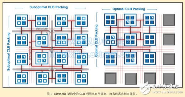
Sounds clear, isn't it? Necessity is the driving force behind the new invention, and it is time to take action on the UltraScale density. The CLB in the UltraScale architecture has been redesigned so that the Vivado® design suite can more efficiently route logic into the CLB. The logic module design makes the alignment more compact, so the wiring resource requirements between CLBs become less. The routing path also becomes shorter. Changes to the CLB in the UltraScale architecture include: adding dedicated inputs and outputs for each flip-flop in the CLB (so that the flip-flops can be used separately for higher utilization); adding more trigger clocks to enable; moving for CLB The bit register and the distributed RAM component add an independent clock. Conceptually, the improved CLB usage and arrangement is shown in the block diagram in Figure 1.

This example shows that a circuit module that previously used 16 CLBs is now implemented with nine modified UltraScale CLBs. The distribution of blue squares and triangles in the figure indicates that the utilization of CLB has increased, and the reduction in red lines indicates that the demand for the number of wires is also decreasing.
Step 2: Add more routing resources.
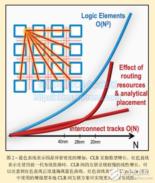
The results in this case will decrease rapidly, unless measures are taken to resolve the issue. For the UltraScale architecture, the solution involves adding more local routing resources so that the routable performance can be increased more quickly as the CLB density increases. Figure 2 shows the result.

However, simply adding hardware routing resources is not enough. You must also reinforce the layout and routing algorithms of your design tools so that they can take advantage of these new resources. The Xilinx Vivado Design Suite has been upgraded accordingly.
Step 3: Handle the increasing clock skew.
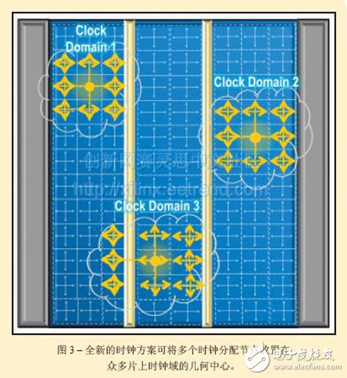
You may not know that the past FPGA clock distribution is too simple. Early generations of FPGAs clocked all on-chip logic by relying on a central clock distribution hub fanned out by the IC geometry center. This global clocking scheme does not work in ASIC-level FPGAs such as the Virtex UltraScale and Kintex UltraScale All Programmable device families. Increasing CLB density and increasing clock rates do not allow this. Therefore, the UltraScale device uses a completely improved clocking scheme, as shown in Figure 3.

The UltraScale architecture's clock distribution network includes a regionalized segmented clocking infrastructure that places multiple clock distribution nodes in the geometric center of many on-chip clock domains. An independent clock distribution node drives an independent clock tree built from an appropriately sized infrastructure segment. This approach has at least three main advantages:
1. The clock skew is rapidly reduced;
2. The available clock resources have increased significantly;
3. Timing closure becomes easier at once.
However, this is not enough to improve the clock infrastructure unless the design tool can support the new clocking scheme. To this end, the Vivado Design Suite has been upgraded accordingly as it is designed for the improved inter-CLB cabling discussed in Step 2.
Xilinx must make major changes to the hardware architecture and design tools for each of the three steps above. This is what Xilinx refers to for collaborative optimization of the UltraScale architecture and the Vivado design suite. This requires a lot of effort and is definitely a must for ASIC-level All Programmable device combinations.
Screen Protector,Uv Glue Screen Protector,Uv Tpu Film Screen Protector,Uv Curing Screen Protector
Shenzhen TUOLI Electronic Technology Co., Ltd. , https://www.hydrogelprotectors.com