On September 13, Apple released three new iPhones. At the same time, Apple's new-generation processor A12, which has received much attention, was officially exposed. Judging from the information officially announced by Apple, the A12 is very powerful. So how does his performance compare to Huawei's just released Kirin 980 and the previous Android flagship processor Qualcomm Snapdragon 845?
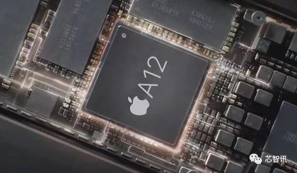
Yesterday, foreign media AnandTech published an analysis article on Apple's A12 processor. AnandTech also quoted TechInsights’ disassembly diagram of Apple’s A12, analyzed the internal structure of Apple’s A12, and also conducted performance tests on A12. They believe that Apple’s official A12 performance improvement data is conservative. The strength is actually stronger. Let's look at it together:
The internal structure of Apple A12 is more complicated
In addition to the performance test, AnandTech also quoted TechInsights's dismantling diagram for Apple A12, and analyzed the internal structure of Apple A12:
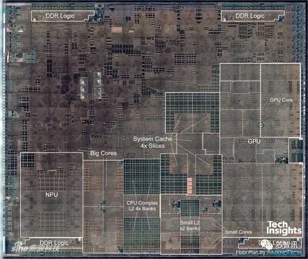
â–²A12 internal structure diagram
In the above A12 internal structure diagram, the leftmost is the NPU core, and the rightmost we can see the four GPU cores of the A12, and the middle is the system cache divided into four blocks. The six CPU cores of the A12 are located in the lower middle part of the above picture. Two Vortex CPU cores are on the left, four large second-level caches are in the middle, and four Tempest CPU cores and their own second-level caches are on the bottom right. Cache.
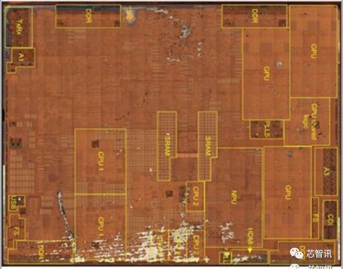
â–²A11 internal structure diagram
Compared with the internal structure of Apple's A11 chip, the internal design of A12 has changed a lot. The NPU core is placed on the far left, and the area occupied by the SoC has also increased significantly. Apple claims that its NPU has changed from the dual-core design in the A11 to the new 8-core design. Due to the addition of a GPU core, the area occupied by the A12's GPU has also further increased. In addition, you can see that the SRAM system cache in A11 is divided into two blocks, while A12 is divided into four blocks, which indicates that the system cache performance of this block has undergone great changes.
In general, the internal structure of Apple A12 has undergone tremendous changes compared to the past. AnandTech claims that the system cache change of A12 is the biggest change since the launch of A7.
In addition, it needs to be added that the single GPU core area of ​​the A12 is reduced by 37% compared to the A11. Obviously, under the blessing of the new 7nm process, the A12 can further reduce the area while adding an additional GPU core.
NPU area increased by 3.16 times, performance skyrocketed
Since the A12 uses the new TSMC’s 7nm process, the transistor density of the A12 has been greatly increased. From the above comparison of the area data of the various functional modules inside the A12 and the A11, the A12 has stronger performance, but the overall Die The size is smaller than the 10nm A11.
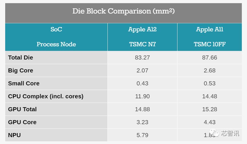
Comparison of the area size data of each functional module inside A12 and A11
In addition, it can be seen that under the support of the 7nm process, the area of ​​the CPU core and GPU core of the A12 is smaller than that of the 10nm A11, but the area of ​​the A12's NPU core has reached 5.79mm², which is the area of ​​the A11's NPU (1.83mm² ) 3.16 times. The soaring area of ​​the NPU core, coupled with the blessing of advanced technology, has led to an increase in the density of transistors per unit area, which has also directly brought about a surge in NPU performance.
According to Apple, the A12's NPU core has a total of 8 cores, with machine learning, multi-precision support and an intelligent computing system. Specifically in terms of performance, compared to the 600 billion operations per second of the previous generation of Apple’s A11 dual-core NPU, the Apple A12’s NPU can perform 5 trillion operations per second (5TFLOPS), with ISP, deep engine, and security isolation. The important components such as zone, video processor, video encoder, storage controller, etc., are more intelligent.
In addition, machine learning (ML, Machine Learning) is one of the most important functions of Neural Engine. The learning ability of Apple A12's CoreML development library is 9 times that of the previous generation, but its power consumption is only 1/10 of the previous generation. Its intelligence is not only reflected in the flexibility and variety of Siri functions, but also in shooting, AR, games (motion tracking and graphics rendering, etc.) and Face ID.
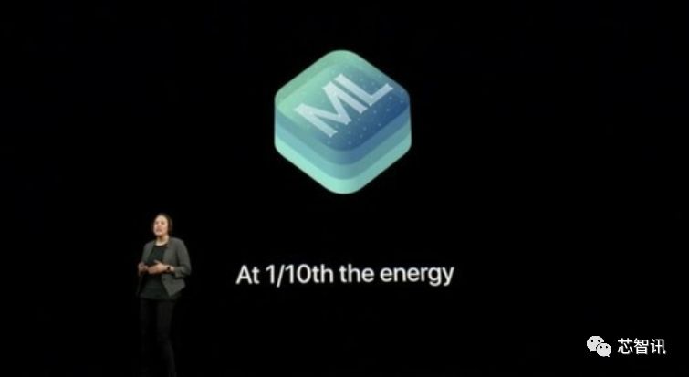
There are rumors that Apple’s A11’s NPU core is based on CEVA’s IP, but this rumor has not been confirmed because Apple does not want the outside world to know.
New cache design
As mentioned earlier, the A12 has made major changes in the system cache, and at the same time the first and second level caches of the large and small core CPUs of A12 have also changed.
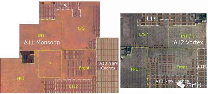
Image source: TechInsights Apple A12Die Shot, ChipRebel Apple A11Die Shot
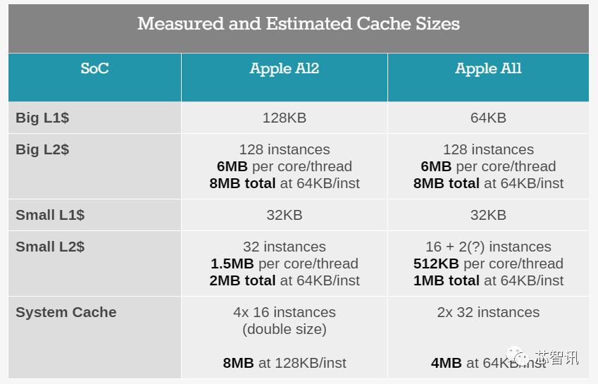
As can be seen from the above figure, the A12 Vortex CPU core's L1 cache accounts for twice that of A11. According to AnandTech's speculation, the L1 cache in A12's Vortex large-core CPU has also doubled compared to A11, from 64KB to 128KB. The second-level cache of Vortex large-core CPU is consistent with that of A11.
So what exactly does Apple's cache hierarchy look like? By looking at the memory latency behavior under different test depths, it can be clearly seen that the level 1 cache L1 has increased from 64KB to 128KB (it is a straight line with no delay). However, AnandTech found a strange phenomenon. In the range of 3MB, the delay increased slowly, until about 6MB. It should be noted that this behavior occurs only when accessing in a completely random mode. In a smaller access window, the delay curve is flat until 6MB, and if it exceeds 6MB, it shows a nearly straight upward trend. In addition to the system cache, AnandTech believes that the overall system cache has not only doubled the number of slices, but also increased its capacity from 4MB to 8MB.
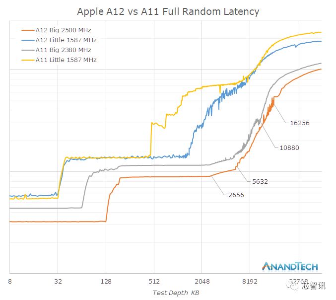
In terms of small CPU cores, from the test point of view, the callable secondary cache of a single small CPU core of A11 seems to be limited to 512KB, while that of A12 has risen to 1.5MB. However, AnandTech is deceived by the power management strategy of the cache. You can see the A11 Mistral core delay, which has a significant jump from 768KB and 1MB, while the A12 core can also see a similar jump at 2MB. In fact, the overall L2 cache of the small CPU core of A11 is 1MB, while that of A12 is 2MB.
It should be pointed out that the working principle of the cache is that when the CPU wants to read a piece of data, it first searches it from the cache, if it finds it, it reads it immediately and sends it to the CPU for processing; if it does not find it, it uses a relatively slow speed from the memory Read and send it to the CPU for processing, and at the same time transfer the data block where the data is located into the cache, so that the entire block of data can be read from the cache in the future, without the need to call the memory.
From the above analysis, we can see that Apple's cache system is very powerful. Compared with the A11, the A12 system has doubled the cache size. In actual operation, there is about 16MB of available cache hierarchy on the large CPU core, which is far superior to other competitors. The increase of the cache will greatly save the time for the CPU to directly read the memory, will make the CPU processing speed faster, and at the same time can reduce energy consumption to a certain extent.
CPU performance comparable to the 6th generation Core?
According to Apple’s official information, the A12 is based on TSMC’s 7nm process and has a built-in six-core CPU, including two performance cores and four efficiency cores. Among them, the performance core has increased by 15% compared to the previous generation, and the power consumption has been reduced by 40%; while the efficiency core has reduced power consumption by 50%.
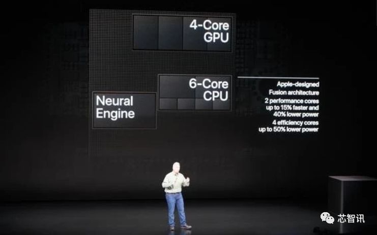
According to AnandTech's test data, the A12's CPU uses two Vortex 2.5GHz large cores and four 1.59GHz Tempest small cores to form a six-core CPU.
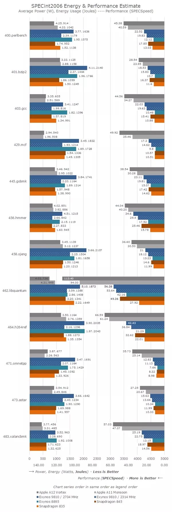
At present, the power consumption ratio of mainstream chips is shown as A12 in dark gray and A11 in light gray. Others include Samsung 9810, Snapdragon 845, etc.
According to the SPECint2006 benchmark test data, the A12 performs on average 24% better than the A11 on the previous generation of devices. The unit energy efficiency ratio (that is, the comparison between computing and power consumption) has increased by 12%, but as the internal cache increases, the power consumption has also increased. The average power consumption of A11 is about 3.36W, and the average power consumption of A12 is 3.64W.
AnandTech's benchmark test shows that the A12's core and architecture improvements are actually "more profound than the improvements officially announced by Apple." It surpasses the Exynos9810 and Snapdragon 845 chips commonly used in the Android camp in terms of performance and power.
AnandTech said that the small gap between the CPU of the A12 and the previous generation of A11 and desktop products is "quite amazing." They also introduced how Apple can improve the performance of old devices through software adjustments. Take the A9 of the iPhone 6s as an example, the highest CPU frequency is 435ms, but the time of iOS 12 is shortened to 80ms, which "greatly improves the performance of interactive workloads." A10 has also made similar improvements (from 400ms to 210ms), but there is no change in A11.
All in all, AnandTech said that the A12 is a "big change" for Apple's processors, with a CPU performance increase of up to 40%. In the SPEC2006int test, the single-thread performance of the A12 is even better than the down-clocked Intel Skylake processor.
GPU performance is twice as high as Snapdragon 845
At the beginning of last year, Imagination publicly stated that Apple plans to no longer use its intellectual property in new products within 15 to 24 months. Therefore, when Apple A11 was launched last year, there were reports that the GPU of the A11 was self-developed by Apple. But in fact, it still seems to be customized based on Imagination's IP. Because its core design is very similar to the previous Rogue of Imagination. In addition, the A12's GPU still supports PVRTC (PowerVR Texture Compression), a proprietary format, which means that the GPU may still be associated with Imagination's IP.
Now, more than 15 months have passed, and Imagination has also been acquired by Chinese investors. Therefore, A12 is expected to use Apple's self-developed GPU.
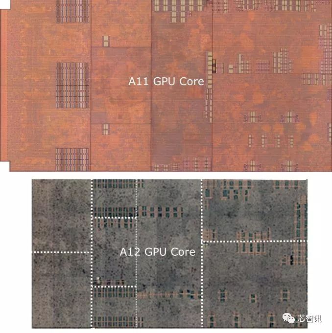
Image source: TechInsights Apple A12Die Shot, ChipRebel Apple A11Die Shot
However, the A12 GPU with model G11P (clocked at more than 1.1GHz) still has some very obvious similarities with last year’s A11 GPU, and its internal functional blocks seem to be largely located in the same location and in a similar manner. structure.
AnandTech said that the biggest progress Apple has made on the A12 GPU is that it now supports memory compression, which alone can significantly improve performance. In the desktop field, GPUs like Nvidia and AMD have supported this technology for many years, and it can improve GPU performance even without increasing memory bandwidth. Similarly, the GPU of a smartphone requires memory compression, not only because of the limited bandwidth on the mobile SoC, but more importantly because of the reduced power consumption associated with high bandwidth requirements.
For example, Arm's AFBC (frame buffer compression technology) technology has always been a technology frequently mentioned in the industry, and Qualcomm and even other manufacturers such as Imagination also have their own related technologies.
Therefore, thanks to the support for memory compression, the support of the 7nm process and the addition of a GPU core, the GPU performance of the A12 has indeed been greatly improved.
According to data released by Apple, the Apple A12 has a built-in 4-core GPU, and its performance is significantly improved by 50% compared to the previous generation (A11 is a 3-core GPU).
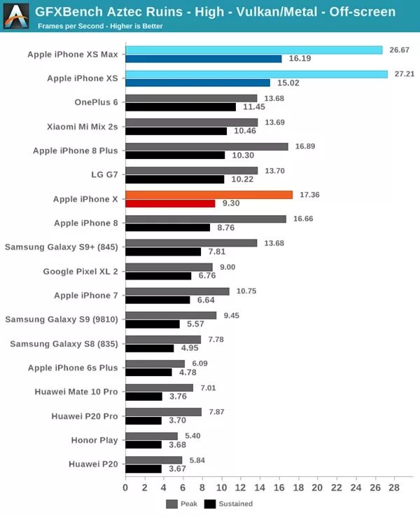
In terms of GPU performance testing, AnandTech uses the GFXBench Aztec Ruins scene as the test benchmark (2K resolution). Under high special effects, it can be seen that the peak performance of the A12 GPU is 61% higher than the previous generation A11, which is a Qualcomm Snapdragon. The performance of the GPU of the 845 is twice that of the Huawei P20 series based on the Kirin 970.
summary:
From the above introduction, it is not difficult to find that compared to the previous A11, the A12 does have a lot of improvements: not only the system cache is redesigned (called by AnandTech as "the biggest change since the introduction of A7"), The CPU core has also been significantly improved, the GPU has begun to support memory compression, and the NPU has also undergone major upgrades, all of which have brought impressive performance improvements.
Portable Energy Storage For Camping
Langrui Energy (Shenzhen) Co.,Ltd , https://www.langruibattery.com