At present, GlobalFoundries (GF) and its partners, including Samsung, Sony, STM (STMicroelectronics), are increasingly investing in FD-SOI.
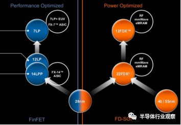
As one of the industry's three largest foundries, GlobalFoundries has been vigorously promoting FD-SOI technology in recent years. The company proposed the 22FDX (22nm process) product plan in 2015 and released the 12FDX (12nm process) platform plan and roadmap at the third Shanghai FD-SOI and RF-SOI Forum held in 2016. The company is also the industry's first manufacturer to introduce the next-generation FD-SOI technology roadmap.
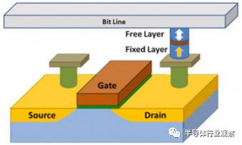
Recently, it is reported that Globalfoundries is researching new non-volatile memory (NVM) technology, which is likely to be used in 22nm FD SOI.

The company's chief technology officer Gary Patton said that Globalfoundries has provided magnetic RAM (MRAM) in its 22FDX process and is currently studying another memory technology option.
The above information was disclosed at the IMEC Technical Forum held in Antwerp last month.
Foundry competitors such as TSMC and Samsung are working hard to introduce advanced 7nm processes that also involve RF circuits and power efficiency. In this case, will Globalfoundries fall behind in the competition of advanced process technology and start to lose customers?
For this issue, Patton emphasized, "We are fully committed to the development of the dual roadmap strategy,"
Patton said that under the guidance of the dual roadmap development strategy, Globalfoundries will tape out 7nm FinFET process products in the second half of 2018, and will achieve production in 2019, and will iterate further in 2019. Patton said the first customers include AMD, IBM and other ASIC design companies.
For Globalfoundries, successful implementation of mass production of FinFET process is very important, because only in this way can we guarantee the capacity utilization rate of its Fab 8 plant in Malta, New York, and bring in revenue with smaller geometric dimensions (such as 3nm) to pay for R & D cost. The company has been investing money in advanced processes, but the short-term return is limited, which puts tremendous pressure on it.
At the same time, another branch of the Globalfoundries dual roadmap, FD SOI, is also competing with Samsung's 28nm FD SOI process, which announced last year that it will launch 18nm FD SOI. In this regard, Globalfoundries said that we are very pleased to see Samsung also participate, which helps to allow more people to enter the market.
Samsung advances to 18FDS
Samsung is an important driving force for FD-SOI. When Moore's Law was developed to the 28nm process node, there was a different situation from the past, that is, from 28nm, and then to higher nodes, such as 20, 16, 14, 10, 7nm, etc., each transistor in each integrated circuit The cost is no longer reduced, but increased.
Therefore, the company believes that the 28nm process is more suitable for the Internet of Things (IoT) in terms of cost, power consumption and performance, especially MCU and sensor products. Therefore, Samsung LSI launched the "28FDS" technology and products, and began mass production in 2016.
The development path of the Samsung Foundry business unit is mainly divided into two, starting from the 28nm node, one is to continue to develop in accordance with Moore's Law, and constantly improve the FinFET process node, from 14nm to the current 10nm, and then turn to the next 7nm.
Another line is the FD-SOI process. The company also uses its technology and scale advantages in memory manufacturing to focus on creating eMRAM to meet future market demands.
In fact, Samsung is an early starter in MRAM R & D. It started this work in 2002 and started the STT-MRAM R & D in 2005. After that, it continued to evolve. In 2014, 8Mb of eMRAM was produced. .
Samsung 28FDSOI embedded NVM has two stages. The first is risk production of electronic money before the end of 2017, and the second is risk production of eMRAM before the end of 2018. And also provide eFlash and eMRAM (STT-MRAM) options.

When the foundry carries out risk production for customers, the process and design may still change to optimize performance and increase output. Since the manufacturing process has not yet been finalized, such production is at the customer's risk. The risky production phase may take several months, which means that eFlash will be available in volume in 2018 and eMRAM will be available in volume in 2019.
Providing 28nm embedded non-volatile memory is challenging. The accepted view is that converting flash memory to 28nm is unrealistic, and other options such as MRAM, phase change memory (PCM) and resistive RAM (ReRAM) lack engineering maturity.
Problems with eFlash include difficulties in 28nm durability and power consumption.
This may be one of the reasons why Samsung launched eFlash first, but customers are expected to use STT-MRAM for a long time. Due to the process advantages of CMOS, MRAM is the most popular in the long run.
Samsung developed the industry's first eMRAM test chip with 28FDS technology in 2017.
In addition, according to ES Jung, general manager of Samsung Foundry business, the company is no longer sticking to 28FDS as it was in 2016, but is starting to move towards 18FDS (18nm FD-SOI). It seems that Samsung's optimism about SOI has continued to increase, and it is estimated that this year will see the introduction of updated SOI products.
Business risk
Regarding commercial risks, Patton said that FD SOI already has sufficient anti-risk capabilities. "Now, the roadmap is not a problem, and IP availability is not a problem, so the risk has been minimized. Another measure is our FDXelerator partner program, which was launched with 7 partners in the third quarter of 2016. It has been increased to 47. Our latest goal is to increase the number of partners to 75 by the end of this year. We have performed several real IC tapeouts on 22FDX instead of test chips. We expect to achieve 12FDX by 2020 Streaming and delivering to customers in 2021. "
Patton emphasized that the radio frequency components and millimeter wave circuits on the FD SOI are world-class, which makes the process very suitable for automotive radar. In fact, its 22FDX process has just obtained AEC-Q100 level 2 production certification. As part of the AEC-Q100 Grade 2 certification, the device must successfully withstand the reliability stress test for a long time in a wide temperature range.
It is reported that Globalfoundries also provides an AutoPro platform to help customers migrate their automotive microcontrollers and ASSP to 22FDX, and make full use of RF and mmWave functions, as well as logic, non-volatile memory (NVM) and high voltage equipment.
ST PCM based on FD SOI
Globalfoundries has been focusing on embedded MRAM, but other companies are offering alternatives. For example, Samsung offers embedded MRAM and flash memory options on its 28nm FDSOI, STMicroelectronics has selected phase change memory (PCM) on 28nm FDSOI, And realized the sampling of high-end microcontrollers for automotive applications. Marco Monti, President of ADG of STMicroelectronics, revealed the news in a speech at ST Financial Analyst Day in London.
It is reported that STMicroelectronics' upcoming microcontroller for electronic control unit (ECU) will contain up to six Cortex-R52 processor cores, with a running frequency of up to 400MHz and an embedded PCM speed of 16 or 32Mbytes.
Monti describes the technology as a "disruptive technology", a 6-core chip with a high clock frequency can provide 15 times the performance of a typical single-core ECU.
Monti said samples have been provided to a major automotive customer.
At the same time, according to reports, TSMC is offering variants of MRAM and ReRAM as embedded memory in its 22nm FinFET process. TSMC will provide embedded ReRAM in 2019.
The report said that these two technologies will be used for 22nm FinFET process technology.
TSMC takes eMRAM and eReRAM
TSMC will provide eMRAM with Samsung and Globalfoundries on 28nm CMOS and 22nm FDSOI processes, respectively, and then achieve a leap with ReRAM products in 2019. Neither Samsung nor Globalfoundries took any action to switch to embedded ReRAM.

Figure: According to a report from the China Economic Daily (EDN), TSMC plans to provide embedded MRAM as a non-volatile memory option for SoCs in 2018, and embedded resistive RAM in 2019.
According to Jack Sun, chief technology officer of TSMC, TSMC plans to use "risk production" of eMRAM chips in 2018, and production of eReRAM chips using a 22nm process in 2019.
Samsung has seen the 28nm eMRAM used by NXP Semiconductors. Globalfoundries' 22FDX eMRAM was originally planned to be provided to customers for prototype design in 2017 and mass production in 2018.
Detailed information about ReRAM is not included in the ReRAM report provided by TSMC, but the company has published many ReRAM papers based on metal oxide structures.
In particular, TSMC has reported that high-k hafnium dioxide dielectric materials used in 16nm FinFET high-k metal gate (HKMG) can also be used as resistance memory devices. Although the first author of the IEDM 2015 paper comes from Tsinghua University in Taiwan, it is also due to the multiple authors of TSMC.
The next stop of the process
"We are studying other non-volatile memory options," Patton said, but he declined to disclose more information. It is worth noting that STMicroelectronics has chosen PCM and Globalfoundries as its FDSOI foundry partner, but Patton seems not enthusiastic about it. Fabless chip design companies are issuing a large number of resistive RAM options for foundry partners. Patton said: "22FDX will be a long-lived node, so I hope to improve many technologies."
Speaking of changes in the market, Patton said that the plan to use extreme ultraviolet lithography (EUV) technology for the 7nm process in 2019 has not changed. "We have two EUV production facilities in Malta, New York. In addition, we can add two. Our third machine is already being upgraded at Veldhoven, ASML headquarters."
Although EUV has made progress in light sources, it still needs to carry out research work on luminous flux and line edge roughness processing throughput and masks, because there are still concerns such as mask defects and the development of 205W compatible protective films.
It is reported that Globalfoundries will launch optical immersion lithography technology, which will be able to provide performance enhancement for 7nm technology. The company believes that FinFET 14nm and 7nm are "main" nodes, skipping 10nm.
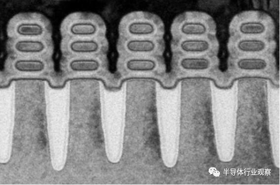
The industry believes that 5nm is another transition node, and 3nm is likely to be the next complete node. 5nm may be the last FinFET node, while 3nm will require a lot of transistor engineering. This will be a huge expenditure for real node improvement. Nanosheets (flat horizontal nanowires, each with nanowire fins surrounded by gates) may be candidates for the 3nm process node. This is Samsung's just announced GAA process technology launched in 2022 or later.
Last month, on the Samsung Technology Forum SFF 2018 USA held in the United States, Samsung announced that it will continue to enter the 5nm, 4nm, and 3nm processes. Among them, the 4-nanometer process will still use the existing FinFET manufacturing technology, which is used in Qualcomm Snapdragon 845 and Samsung Exynos flagship chips. But at the 3nm process node, Samsung began to abandon the FinFET technology and adopt GAA (Gate-All-Around) nanotechnology.

Figure: Samsung Electronics has announced a roadmap and updated its process nodes, and introduced a 3 nanometer full gate (GAA), which will be launched in 2022 or later.
Gate-All-Around is to surround the gate. Compared to the current FinFET Tri-Gate tri-gate design, the underlying structure of the transistor will be redesigned to overcome the physical and performance limits of the current technology, enhance gate control, and greatly improve performance. Samsung's GAA technology is called MBCFET (Multi-Bridge Channel Field Effect Transistor) and is being developed using nano-layer devices.
Conclusion
Feature size scaling is becoming slower and slower, and 3nm technology will mature three to four years after mass production at 7nm. Starting from 7nm, further research is like playing an extreme sport, especially like extreme sports at high altitude, the air will become thinner and more difficult.
Electric Foot Warmer,Electric Heated Foot Warmers,USB Heated Foot Warmers,Office Electric Foot Warmer
Ningbo Sinco Industrial & Trading Co., Ltd. , https://www.newsinco.com