First, the source of conduction EMI generated by switching power supply
1, test line conducted EMI FIG.
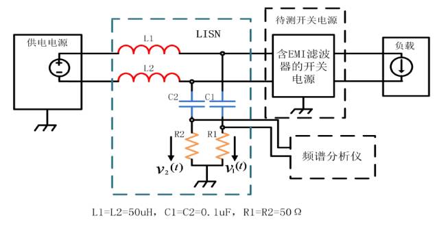
LISN—Line Impedance Stabilization Network Source impedance stabilization network (artificial power network).
LISN is an important auxiliary device in electromagnetic compatibility in power systems. It can isolate network disturbance, to provide a stable test impedance, and filtering functions.
LISN is a network that is added between the grid and the equipment under test in order to objectively assess the interference of the equipment under test (DUT) during the conducted interference emission test . The network has the following features:
1) Provide a specified stable line impedance within the specified frequency range. Because the power grid is affected by various factors, its line impedance is unstable. However, in the measurement of conducted interference, impedance is very important. In order to use the voltage method to have a uniform test condition in the measurement of the conducted emission voltage, a stable line impedance is artificially prepared. Typically 50Ω network impedance is provided in the RF section.
2) , LISN isolates the grid from the equipment under test. The power supplied to the DUT must be pure. Otherwise, the grid will inject interference into the DUT, and the EUT will also introduce interference into the grid, which will make it unclear on the EMC analyzer which is the interference on the EUT. Therefore, only by isolating the two, the measurement results are valid.
3) Use the high-pass filter of the LISN to couple the interfering signals generated by the DUT to the EMC analyzer and prevent the grid voltage from being applied to the EMC analyzer. The power supply can be either DC or AC. The figure is represented by a DC voltage source and the load is represented by a DC current source.
A: In the low frequency band of the power supply, the above EMI test circuit can be equivalent to:
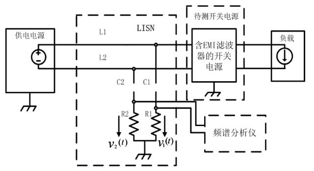
At this time, L1 and L2 may be equivalent to a short circuit, C1, and C2 may be equivalent to an open circuit, low frequency current (power stream portions) does not flow into the two test resistors LISN, LISN point does not affect the normal operation of the switching power supply.
B: In the frequency band specified by the EMI standard, the above EMI test line can be equivalent to:
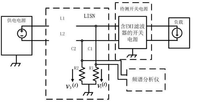
At this time, L1 and L2 can be equivalent to open circuit, C1 and C2 can be equivalent to short circuit, and the input voltage source and load without high frequency component can be equivalent to short circuit and open circuit respectively. The switching power supply is equivalent to its EMI equivalent circuit. The EMI generated by it does not flow into the input due to the presence of the LISN, but flows directly into the two resistors of the LISN. The equivalent circuit is as follows:
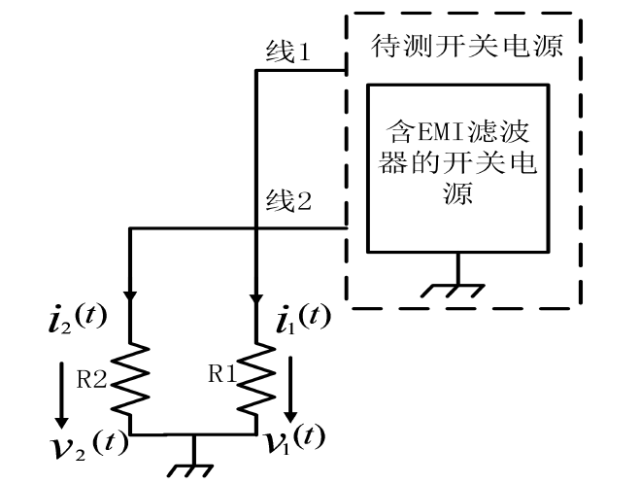
The voltage across resistor R1 and resistor R2 can be labeled as follows:

V1(t) and V2(t) are the EMI noise voltages on line 1 and line 2, respectively. The spectrum is marked by the test in dB/uV. From this equivalent circuit, it can be judged that the switching power supply generates conducted EMI. The root cause is the high frequency source in the switching power supply and the impedance to the path of the load. The differential mode noise of an actual AC power source is generated by a swaying (pulsating) current - but the differential mode noise source is more similar to a voltage source (the current forms a certain voltage across the impedance). On the other hand, common mode noise is caused by the swaying voltage (a rapidly changing voltage creates a rapidly changing current on the parasitic capacitance), but the common mode noise source is more like a current source. This is why common mode noise is more “stubborn.†Like any current source, they require a circulating circuit. Because the path includes the rack, the enclosure becomes a high frequency antenna.
2, the source of conductive EMI
A conductive EMI equivalent circuit for a switching power supply can be represented by the following general structure:
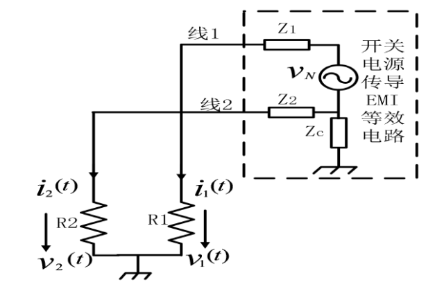
From the conducted EMI equivalent circuit, there are three sources of conducted EMI, one is the EMI source (in the switching power supply, often the AC component in the voltage or current waveform of the power switching device), and the other is the EMI path (with specific topology). Related), another one is the load of EMI. The EMI load in the equivalent circuit is a fixed 50Ω resistor, which is the EMI source and EMI path (equivalent to EMI impedance). How to determine the different power converters, and so on different control mode switching power supply of the conductive EMI is achieved equivalent circuit analysis and design of key conducted EMI filter, but also know the force suppressing means have conducted EMI.
Second, the conduction EMI equivalent circuit of the switching power supply
2. Conductive EMI equivalent circuit of flyback switching power supply
(1) Circuit schematic
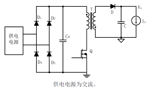
(2) Two working modes
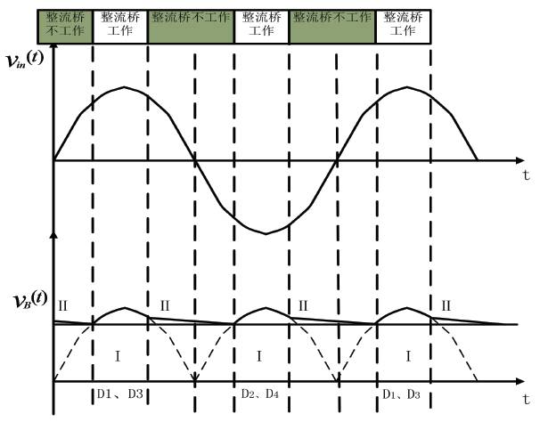
In half of the grid cycle, the input rectifier bridge has two large operating modes, namely: rectifier bridge operating mode I and rectifier bridge inactive mode II.
(3) EMI equivalent circuit derivation of working mode I
3-A, the equivalent circuit of the working mode I (the same as the positive and negative half cycles)
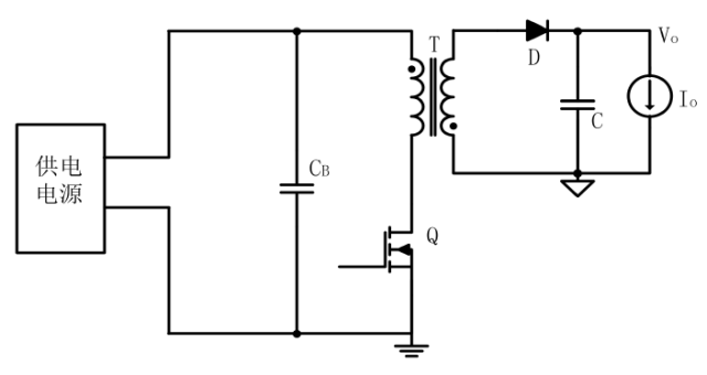
In the case of the working mode I, the two working modes will appear in both positive and negative half cycles, and the rectifier bridge is turned on.
3-A-1: Equivalent circuit of working mode I in the presence of LISN
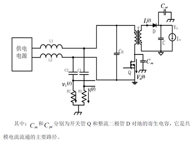
3-A-2: Equivalent controlled source circuit for operating mode I with LISN
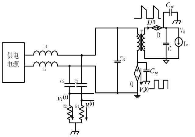
The time-varying factors and non-linear factors of the switching converter are mainly caused by the switching elements. In order to make the equivalent circuit becomes a linear converter circuit, the switching element average model method taken directly switching element method analysis of.
First , the voltage or current variable of the switching element is averaged in one switching cycle, and the switching element is replaced by the controlled source whose average variable is the parameter, and an equivalent average parameter circuit is obtained. The average parameter equivalent circuit eliminates the ripple caused by the switching action in the variable waveform, that is, eliminates the time-varying factor, but is still a nonlinear circuit. Such a circuit is called a large signal equivalent circuit because it contains both a DC component and an AC component.
Secondly , if the average variable in the large-signal equivalent circuit is equal to its corresponding DC component, and the inductance is equivalent to a short circuit and the capacitance is equivalent to an open circuit in the steady state of the DC circuit, the DC equivalent circuit of the converter can be obtained. The DC equivalent circuit is a linear circuit; if the average variable in the large signal equivalent circuit is decomposed into the sum of the corresponding DC component and the AC small signal component, the disturbance is separated, and the product term of the small signal component is ignored (ie, two The small amount of the order is linearized, and then the DC amount in each variable is removed, and the small signal equivalent circuit of the converter can be obtained, and the small signal equivalent circuit is also a linear circuit. It can be seen that the guiding idea of ​​the average model method of the switching element is still to average, separate the disturbance and linearize.
In the above figure, the switch Q is equivalent to a controlled voltage source, and the rectifier diode D is equivalent to a controlled current source. There sometimes supply switch Q is turned on is the input voltage Vg, sometimes the short circuit, the input voltage with the average value of the state variables characterizing the active terminal voltage of the switching element Q is reasonable, therefore controlled by a voltage controlled voltage source instead of the active switch Q; sometimes passive switch D is turned on secondary winding current, sometimes open, since the inductor current is a state variable, the average value of the average current in the inductor current characterization passive switching element D is reasonable, Therefore, the passive switching element D is replaced by a current controlled controlled current source.
3-A-3: Equivalent controlled source averaging circuit (DC equivalent) for operating mode I with LISN
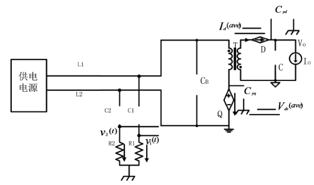
In the DC equivalent circuit diagram above, the inductors L1 and L2 are equivalent to a short circuit, and the capacitor is equivalent to an open circuit.
3-A-4: Equivalent controlled source averaging circuit (AC equivalent) for operating mode I with LISN
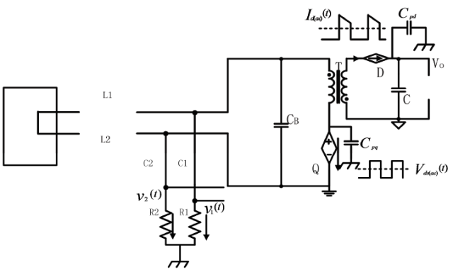
In the AC equivalent, the output load and the inductor are equivalently open, and the capacitor and the power supply are equivalently short-circuited. As can be seen from the figure , the AC component V ds(ac) (t) of the switching transistor Q and the AC component I d(ac) (t) of the diode D can be Fourier transformed and decomposed into sine waves of different frequency components. The frequency is different, the impedance is also transformed, and the spectral amplitude formed by the different frequency components is added by the superposition principle.
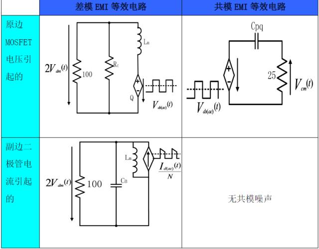
3-B-1: EMI equivalent circuit of operating mode I under the action of the primary MOSFET AC voltage component
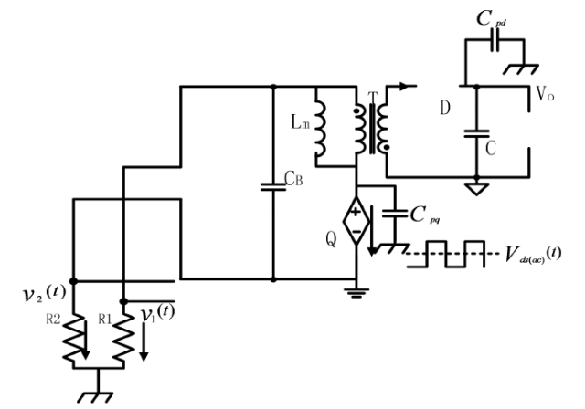
Under the action of the MOSFET AC voltage component, the secondary current source is open. Since the secondary current flows through zero, the primary current is also zero. In this case, the transformer does not work. Only the excitation inductance Lm simplifies the above circuit diagram. The equivalent circuit diagram is:
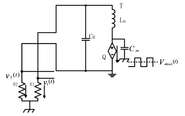
Under the action of the MOSFET alone, the differential mode component path is:
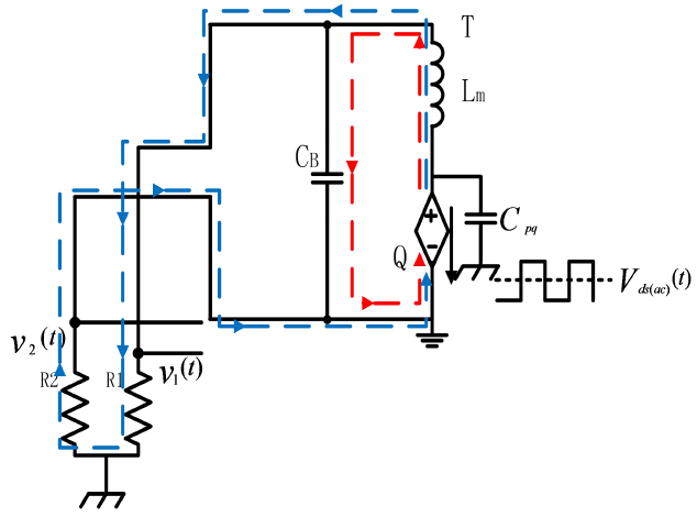
Among them, the differential mode component is divided into two branches, one as shown in red and the other as blue. In the equivalent circuit in such a filter capacitor CB to a slip differential mode component provides a path can be known if the CB filter capacitor to reduce the impedance of the differential mode component more shunt, the voltage formed by resistors R1 and R2 It will be smaller, and the instrument detection amplitude is lower. Generally, we select the filter capacitor with the equivalent series impedance. In the other branch , there is a magnetizing inductance Lm. From the viewpoint of suppressing the differential mode component, increasing the value of the magnetizing inductance Lm can increase the impedance and also have a good inhibitory effect on the differential mode component.
Under the action of the MOSFET alone, the common mode component path is:
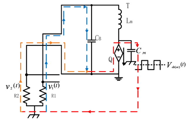
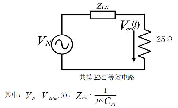
It can be seen that in order to effectively reduce the common mode component, it is necessary to reduce the capacitance of the parasitic capacitance Cpq and increase the effective impedance of the common mode flow path.
The final EMI equivalent circuit of the operating mode I under the action of the primary MOSFET AC voltage component is:
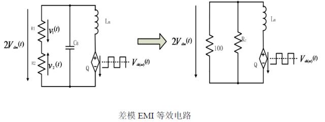
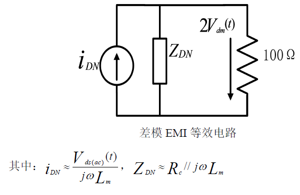
In the differential mode EMI equivalent circuit, the resistors R1 and R2 in series with a current flowing through the differential-mode voltage is generated at both ends of the resistor R1 and the resistor R2 are electrically Vdm (t), so that the equivalent series resistance of resistors R1 and R2 A resistance of 100 Ω produces 2 Vdm(t). The greater the inductance of magnetizing inductance Lm differential mode suppression better, the modulus of the difference is divided, the CCM mode is better than differential mode DCM.
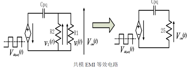
EMI final equivalent circuit of working mode I under the action of the primary MOSFET AC voltage component
3-B-2: EMI equivalent circuit for operating mode I under the action of the alternating current component of the secondary diode.
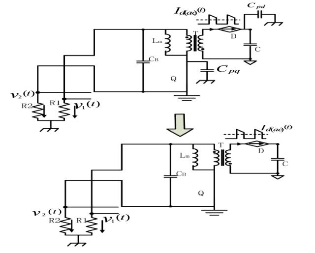
In the case of low frequency (150KHz), the parasitic capacitance of the transformer is ignored (the inter- layer capacitance of the transformer and the primary and secondary capacitances cannot be ignored at high frequencies ). Since the rectifier diode to ground capacitance cannot form a common mode loop, there is no common mode noise on the LISN load.
EMI final equivalent circuit of working mode I under the action of the secondary current diode alternating current component
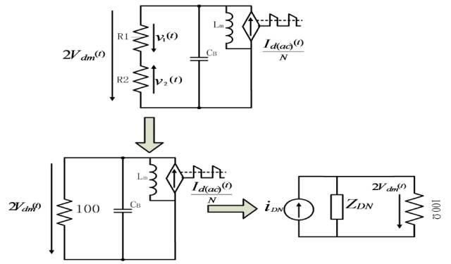
Differential mode EMI equivalent circuit

Since the secondary-side diode-to-ground parasitic capacitance cannot form a common-mode loop at low frequencies, there is no common- mode EMI equivalent circuit.
(4) EMI equivalent circuit derivation of working mode II
4-A: Equivalent circuit of working mode II-I
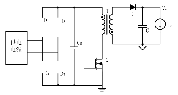
â…¡ in the working mode, when the D1-D4 are turned off, not in LISN conducted EMI noise, seen from the surface of the test an equivalent circuit of EMI, because there is no noise path, conducted EMI noise is not generated. This mode of operation can also be referred to as working mode II-I.
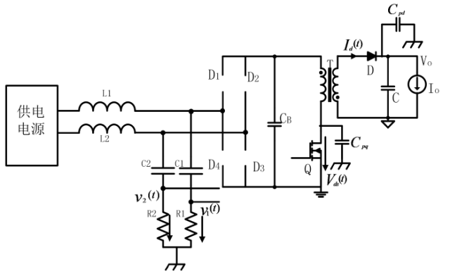
4-B: Equivalent circuit of working mode II-II
In the operating mode II, one of the diodes in D1-D4 is turned on, and the other three diodes are turned off . In this case, the EMI equivalent circuit is different from the equivalent circuit when the diode is all turned off, and the operating mode is different. The EMI equivalent circuit in I is different. This condition is called II-II (non-inherent differential mode noise).
Reason: when the switching voltage changes, there will be a momentary capacitor charge-discharge current, a current flows through this branch Cpq, the earth and the LISN, the maximum current can not open a through-diode rectifier bridge, its situation As mentioned earlier, the four diodes in the rectifier bridge are cut off and no noise is generated;
When this current turns on a diode in the rectifier bridge (such as diode D1 when 0 < V AB < V CD ), the other diodes will be turned off due to reverse bias. When this current is reduced to zero, diode D1 should be off, when, due to rectifier bridge diodes are very slow, it can not be turned off in the switching cycle, so as to cause the diode in the 0 <V AB <V CD has been turned on; this rectifier bridge, while not working, but the There is a diode that is conductive.
The following does not work, but there is a bridge rectifier diode is turned on (conducting assuming D1) of the equivalent circuit analysis EMI.
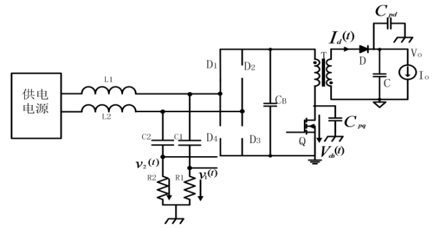
4-B-1: Equivalent controlled source averaging circuit (DC equivalent) for operating mode II-II with LISN
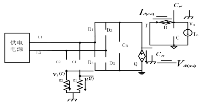
4-B-2: Equivalent controlled source EMI circuit with operating mode II-II in the case of LISN (AC equivalent)
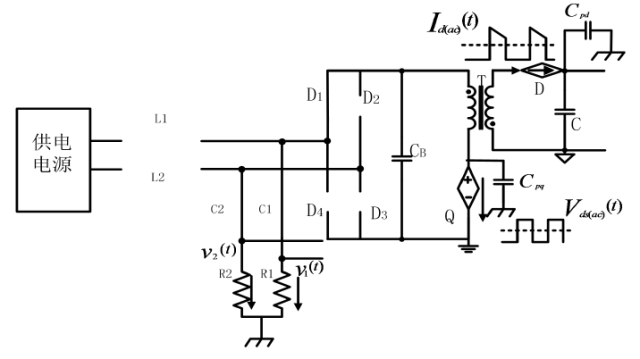
4-C-1: EMI equivalent circuit of working mode II-II under the action of the AC voltage component of the primary MOSFET
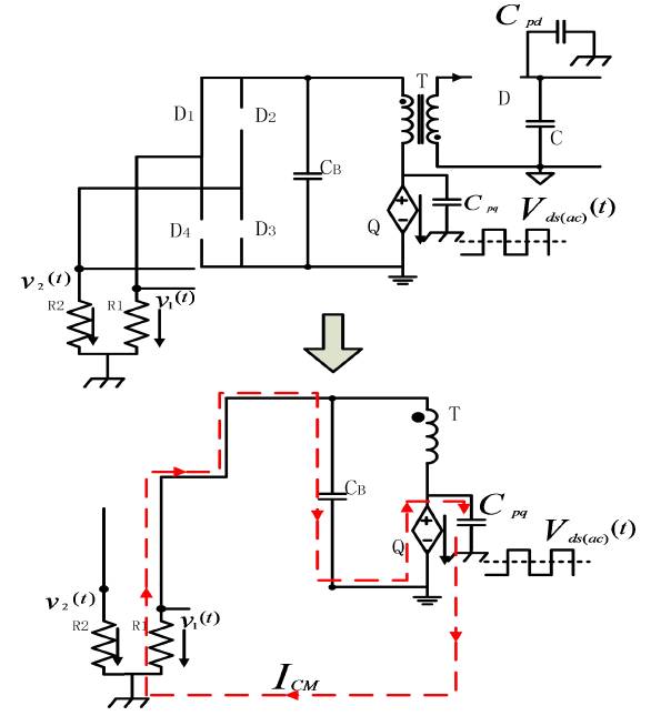
The red dotted line in the above equivalent circuit indicates a common mode loop and no differential mode loop. However, only resistor R1 is noisy and can be practically understood as differential mode noise.
Working mode II-II EMI final equivalent circuit under the action of the primary MOSFET AC voltage component alone
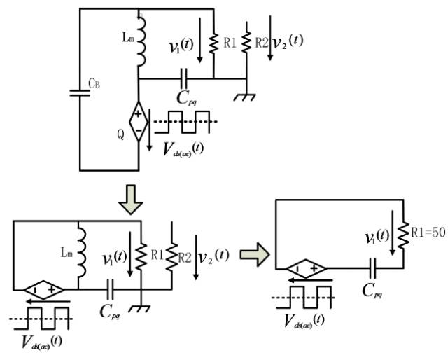
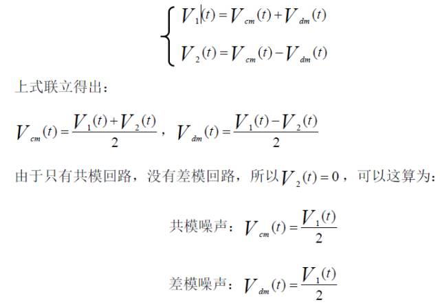
According to the foregoing analysis, a single element path difference acting mode and common mode loop circuit, may be obtained out:
When there is an EMI filter, the differential mode noise in this noise can be converted to common mode noise, such as the equivalent circuit in the 4-C-1 mode of operation, adding the differential mode capacitor Cx.
4-C-1: EMI equivalent circuit of working mode II-II under the action of the AC voltage component of the primary MOSFET
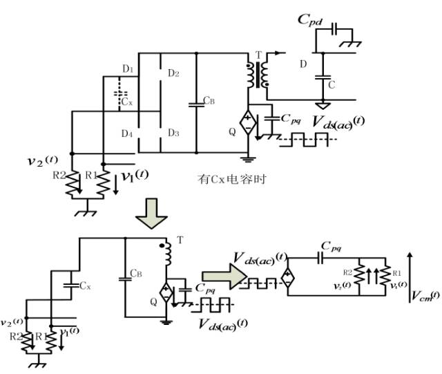
The differential mode noise in Mode II-II can be converted to common mode noise due to the differential mode capacitance Cx in the EMI filter .
4-C-2: EMI equivalent circuit of working mode II-II under the action of the secondary component of the secondary diode
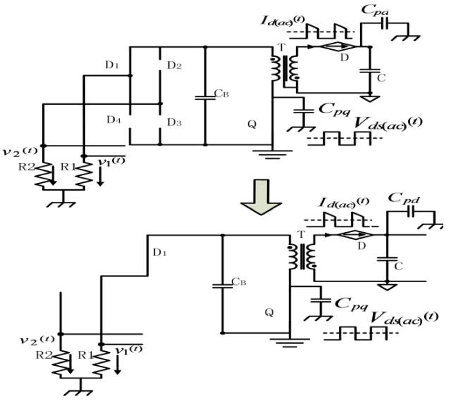
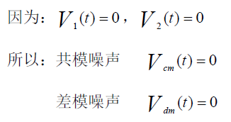
Therefore, in the working mode II-II secondary side diode has no effect on common mode noise and differential mode noise.
discuss:
--- Working mode I is different from conducted EMI in working mode II;
--- If all four diodes in operating mode II are off, the operating mode does not produce any conducted EMI due to the noise-free path ;
--- If there is a diode in conduction mode of operation â…¡, three other diode is turned off, the operating mode of the common mode EMI noise â…¡ and â… substantially the same operating mode, the operating mode and differential mode noise is likely greater than â…¡ â…° differential mode noise operating mode, there may be less than the differential mode noise â…° operation mode, because there is a mode of operation â…± extrinsic differential mode noise present when a diode is turned on;
--- Non-inherent differential mode noise can be completely eliminated by converting the X capacitor in the EMI filter into symmetrical common mode noise;
--- The above EMI equivalent circuit is only the ideal equivalent circuit for EMI low frequency band;
--- The actual EMI equivalent circuit, but also consider the parasitic parameters of the transformer, the lead inductance of the PCB Layout, etc.;
--- considered as an interlayer capacitance of the transformer, a capacitor parameter can be used, when the secondary component of the diode current will generate EMI common-mode noise on the load between its primary and secondary, as it involves EMI filter parameters, It is only necessary to consider the equivalent circuit of the low frequency band, so this factor can be ignored. However , when analyzing the EMI common mode noise in the actual high frequency band, the influence of the AC component of the secondary side diode on the common mode noise through the inter-layer capacitance of the transformer is also considered .
(5) Summary of EMI equivalent circuit of flyback converter under AC input:
5-1: EMI equivalent circuit of operating mode I
5-2-1: EMI equivalent circuit for operating mode II-I
When D1-D4 are off, there is no noise on the EMI load, so there is no EMI equivalent circuit.
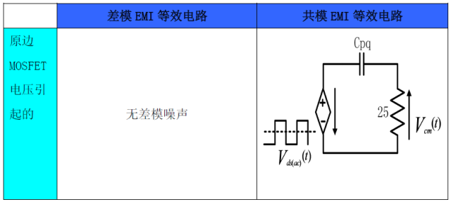
5-2-2: EMI equivalent circuit of working mode II-II
In Operation Mode II-II: When the primary MOSFET voltage acts alone, there is a non-inherent differential mode noise, but it can be converted to common mode noise using the X capacitance in the EMI filter. When secondary diode current acting alone, because no circuit noise, the EMI noise load undetectable, so that the equivalent capacitance added EMI summarizes the X capacitance is:

3. High-frequency equivalent circuit of switching power supply EMI (DC/DC flyback switching power supply)
High-frequency EMI equivalent derivation of DC flyback switching power supply:
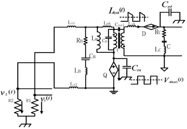
(1) EMI equivalent circuit under the action of the AC voltage component of the primary MOSFET
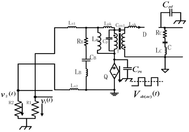
(1) -A: differential mode EMI equivalent circuit under the action of the primary AC voltage component separately from the MOSFET
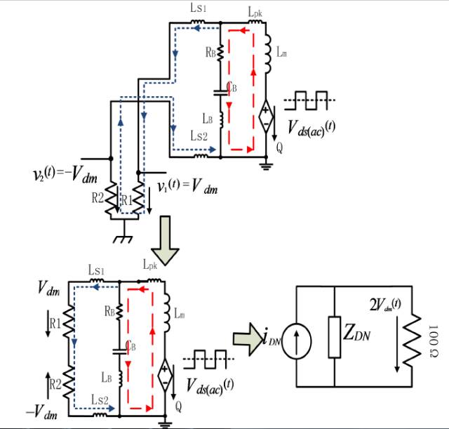
Differential mode EMI in the high frequency equivalent circuit seen, an equivalent circuit of differential mode EMI source voltage waveform and the MOSFET addition, the magnetizing inductance, filter capacitor ESR related, but also with a transformer, the input filter capacitors and other parasitic lead wire The parameters are related. This is very different from the low frequency band, and the same EMI impedance is also very different from the low frequency band.
(1)-B Common-mode EMI equivalent circuit under the action of the AC voltage component of the primary MOSFET
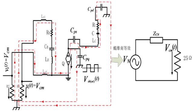
In the equivalent circuit seen from the high frequency common mode EMI, EMI common-mode equivalent circuit in addition to the capacitance between the source and the voltage waveform, the drain of the MOSFET and the heat sink related, but also the interlayer capacitance of the transformer, the diode cathode The capacitance between the heat sink and the parasitic parameters of the filter capacitor are related to the lead inductance and the like. This is very different when the low frequency section, the same EMI impedance is also a great difference between the low frequency band.
(2): EMI equivalent circuit under the action of the secondary current diode alternating current component
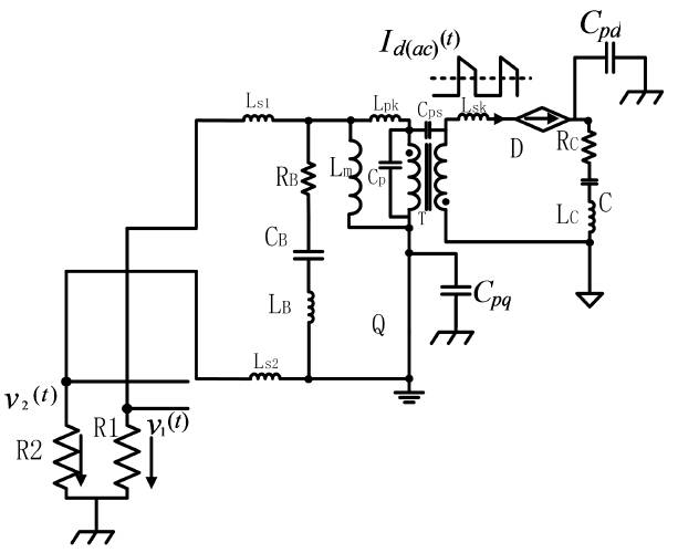
(2)—A: Differential mode EMI equivalent circuit under the action of the alternating current component of the secondary diode
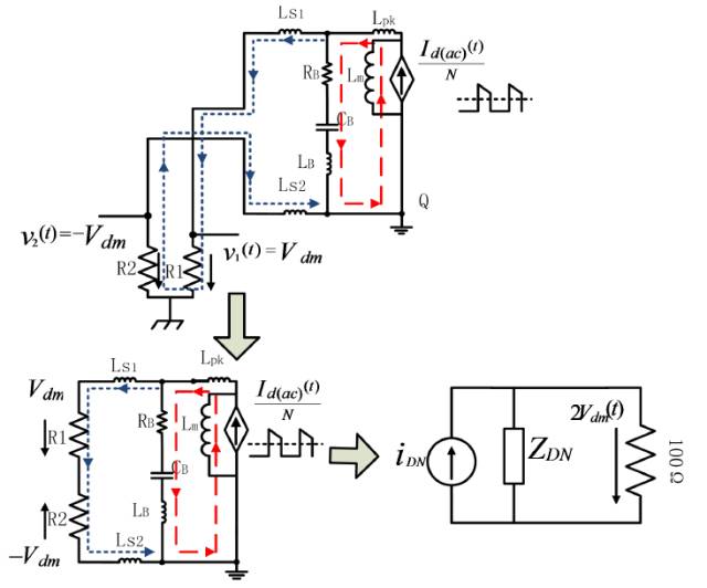
Differential mode EMI in the high frequency equivalent circuit seen, an equivalent circuit of differential mode EMI source and the diode current waveform in addition, the magnetizing inductor, the filter capacitor ESR related, but also with a transformer, the input filter capacitors and other parasitic lead wire related parameters, which are very different and at low frequencies, the same EMI impedance varies considerably with the low frequency section.
(2)—B: Equivalent circuit of common mode EMI under the action of the AC component of the secondary diode
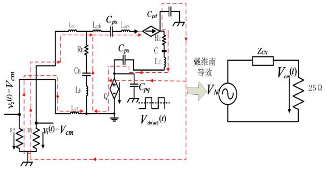
In the equivalent circuit seen from the high frequency common mode EMI, EMI common-mode source in addition to the capacitance between an equivalent circuit of the diode and the secondary current waveform related, but also the interlayer capacitance of the transformer, cathode of the diode and the heat sink And the parasitic parameters of the filter capacitor are related to the lead inductance. This is quite different from the low frequency band (which can be seen as no common mode path) .
Display Port And Mini Display Port
Display Port And Mini Display Port
Display Port ,Mini Display Port
ShenZhen Antenk Electronics Co,Ltd , https://www.antenkelec.com