Most of the isolated driver products use optocouplers to isolate the input drive signal and the driven insulated gate. They are supported by a thick film or PCB process, and some of the RC components are connected by pins. This kind of product is mainly used for the driving of IGBT. Since the IGBT has a current tailing effect, the optocoupler driver is always under negative voltage shutdown. Below we will design the relevant drive circuit based on M57962L!
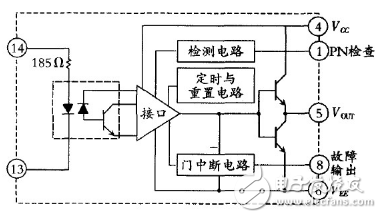
The following figure shows the internal structure of the M57962L driver. The optocoupler is used for electrical isolation. The optocoupler is fast. It is suitable for high-frequency switching operation. The primary side of the optocoupler has series current limiting resistor (about 185 Ω), which can be 5 V. The voltage is applied directly to the input side. It uses a dual power supply structure, integrated with 2 500 V high isolation voltage optocoupler and overcurrent protection circuit, overcurrent protection output signal terminal and TTL level compatible input interface, drive electrical signal delay up to 1.5 Us.

When the M57962L is used alone to drive the IGBT. There are three points that should be considered. First of all. The maximum current rate of change of the driver should be set within the limits of the minimum RG resistance, because for many IGBTs, when RG is used too large, td(on) (on-delay time) is increased, td(off) (cut-off delay time), tr (rise time) and switching loss, this loss should be avoided as much as possible in high frequency applications (over 5 kHz). Also. The loss of the drive itself must also be considered.
If the loss of the drive itself is too large, it will cause the drive to overheat and cause damage. Finally, when the M57962L is used to drive large-capacity IGBTs, its slow turn-off will increase losses. The cause of this phenomenon is that the current flowing to the gate of the M57962L through the Gres (reverse transfer capacitor) of the IGBT cannot be absorbed by the driver. Its impedance is not low enough, this slow turn-off time will become slower and requires a larger snubber capacitor to apply the driver circuit of the M57962L design as shown below.
Circuit Description: Power supply decoupling capacitors C2 ~ C7 use aluminum electrolytic capacitors, the capacity is 100 uF / 50 V, R1 resistance value is 1 kΩ, R2 resistance value is 1.5kΩ, R3 is 5.1 kΩ, power supply uses positive and negative l5 V power supply module Connected to the 4th and 6th pins of the M57962L respectively, the logic control signal IN is input to the driver M57962L via the l3 pin. The bidirectional voltage regulator Z1 is selected to be 9.1 V, Z2 is 18V, and Z3 is 30 V, which prevents the gate and emitter of the IGBT from breakdown and damages the driving circuit. The diode adopts the fast recovery FR107 tube.
IGBT drive design for multi-circuit output

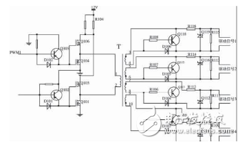
The working principle is as follows: the two inverting PWM signals output by the PWM control chip are amplified by the power amplifying circuit composed of components, and then the four driving signals are isolated and output through the pulse transformer. The four drive signals are divided into two groups of opposite phases according to the trigger phase. The drive signal 1 is in phase with the drive signal 3, and the drive signal 2 is in phase with the drive signal 4. The circuit uses a pulse transformer to achieve reliable isolation of the high voltage main circuit and control loop of the controlled IGBT. The voltage regulator between the GE of the IGBT is used to prevent the interference from generating too high UGE and damage the control pole of the IGBT. Like the MOSFET, a negative bias prevents the gate from being too high due to excessive d/dt. However, as long as the bus voltage transient overshoot is controlled, the negative bias of the IGBT is not required. In this circuit, the secondary circuit of the pulse transformer is connected to the corresponding circuit to cut off the negative pulse of the driving waveform, which greatly reduces the power consumption of the driving circuit.
Since the switching characteristics of the IGBT and the safe working area change with the change of the gate driving circuit, the performance of the driving circuit will directly affect whether the IGBT can work normally. In order to make the IGBT work reliably. The IGBT driver circuit needs to meet the following requirements:
1. A certain forward and reverse drive voltage is provided to enable the IGBT to be turned on and off reliably.
2. Providing a sufficiently large instantaneous drive power or instantaneous drive current enables the IGBT to establish a gated electric field in time and turn on.
3. With as little input and output delay time as possible to increase the operating frequency.
4. High enough input and output electrical isolation to insulate the signal circuit from the gate drive circuit.
5. Sensitive overcurrent protection.
IGBT drive circuit design trends
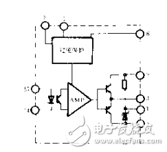
The IGBT gate control circuit composed of the integrated module has been widely used due to its reliable performance and convenient use, and is also the development direction of the drive circuit. All major companies have different series of IGBT drive modules, the basic functions are similar, and various control performances are also constantly improving. For example, Fuji's EXB series driver module has an optical coupling device and an overcurrent protection circuit. Its function is shown in the figure below.

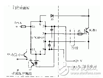
The external interface circuit between the EXB series driver module and the IGBT is shown below. The drive signal is amplified by an external transistor and input to the module by pin 14 and pin 15. The overcurrent protection signal is obtained by measuring the on-state voltage vCE reflecting the current of the component, and then outputting through the external optocoupler device. When the overcurrent is applied, the IGBT is immediately turned off. Two 33uF external capacitors are used to absorb variations in the supply voltage caused by the power wiring. The leads of pin 1 and pin 3 are respectively connected to the emitter E and the gate G of the IGBT, the leads are to be as short as possible, and a twisted wire should be used to reduce interference with the gate signal. In the figure, D is a fast recovery diode.

Since the IGBT is not allowed to turn off too quickly after a short circuit occurs, because the short-circuit current is already quite large, if it is turned off too quickly, it will cause a large di/dt, which will be in the IGBT under the action of the line distributed inductance. Excessively high surge voltage is generated, which can easily damage components. Therefore, after a short circuit occurs, the short-circuit current should be suppressed by reducing the gate positive bias voltage, and then the IGBT is turned off. This is called "slow shutdown technology", a module produced by some companies in this function. Existing applications.
Single Core Armored Cable,Types Of Armoured Cable,Single Core Wire,Armored Cable Power
Shenzhen Bendakang Cables Holding Co., Ltd , https://www.bdkcables.com