1. MOS tube working principle -- Introduction to MOS tube
MOS tube , that is, an insulating field effect transistor in an integrated circuit. MOS English is called Metal-Oxide-Semiconductor, which is metal-oxide-semiconductor. Specifically, this name describes the structure of MOS transistors in integrated circuits, that is, on a certain structure of semiconductor devices, plus silicon dioxide and metal. Forming a gate. The source and drain of the MOS tube are tunable, and are all N-type regions formed in the P-type backgate. In most cases, the two zones are identical, and even if the two ends are reversed, the performance of the device will not be affected. Such devices are considered to be symmetrical.

2. MOS tube working principle - structural characteristics of Mos tube
The internal structure of the MOS transistor is as shown in the following figure; when it is turned on, only one carrier (multi-sub) of one polarity participates in conduction, and is a unipolar transistor. The conduction mechanism is the same as that of the small power MOS tube, but the structure is quite different. The low power MOS tube is a lateral conductive device. The power MOSFET mostly adopts a vertical conductive structure, also known as a VMOSFET, which greatly improves the withstand voltage and current resistance of the MOSFET device. ability.
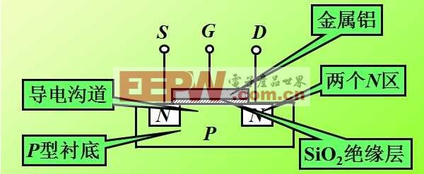
Its main feature is that there is a silicon dioxide insulating layer between the metal gate and the channel, so it has a high input resistance. When the tube is turned on, an n-type conductive channel is formed in two high-concentration n-diffusion intervals. The n-channel enhancement type MOS transistor must have a forward bias applied to the gate, and the n-channel MOS transistor generated by the conductive channel is only available when the gate-source voltage is greater than the threshold voltage. The n-channel depletion mode MOS transistor refers to an n-channel MOS transistor which is formed by a conductive channel when no gate voltage is applied (the gate-source voltage is zero).
3. MOS tube working principle - characteristics of MOS tube
3.1 MOS tube input and output characteristics
For the common source connection circuit, the source and the substrate are separated by a silicon dioxide insulating layer, so the gate current is zero.
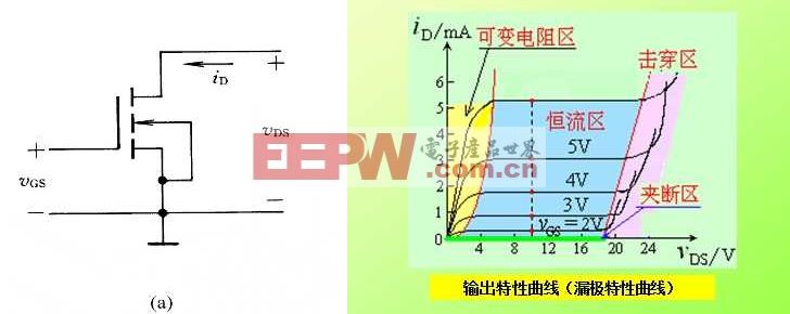
Figure (a) shows the circuit of the common source connection, and the output characteristic curve is shown in the right figure.
When VGS

3.2 MOS tube conduction characteristics
As a switching element, a MOS transistor operates in either a cut-off or a conducting state. Since the MOS transistor is a voltage control element, its operating state is mainly determined by the gate-source voltage uGS. The NMOS tube is taken as an example to introduce its characteristics.
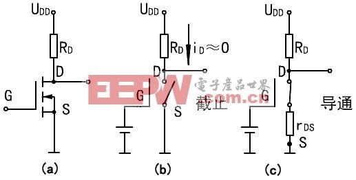
Figure (a) is a switching circuit composed of an NMOS- enhanced tube.
The characteristics of the NMOS , Vgs greater than a certain value will be turned on, suitable for the case when the source is grounded (low-side drive), as long as the gate voltage reaches 4V or 10V.
The characteristics of the PMOS, Vgs is less than a certain value will be turned on, suitable for the case when the source is connected to VCC (high-end drive). However, although PMOS can be conveniently used as a high-side driver, NMOS is usually used in high-end driving because of high on-resistance, high price, and low replacement.
4. MOS tube working principle
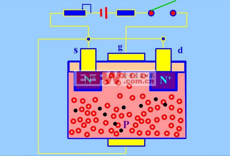
The working principle of MOS transistor (with N-channel enhancement MOS FET) is to use VGS to control the amount of "inductive charge" to change the condition of the conductive channel formed by these "inductive charges" and then achieve control leakage. The purpose of the polar current. When manufacturing the tube, a large amount of positive ions appear in the insulating layer by the process, so that more negative charges can be induced on the other side of the interface, and these negative charges turn on the N region of the high-permeability impurity to form a conductive groove. The channel has a larger drain current ID even when VGS=0. When the gate voltage is changed, the amount of charge induced in the channel also changes, and the width and width of the conductive channel also change, and thus the drain current ID changes as the gate voltage changes.
Knowledge extension
Classification of MOS tubes
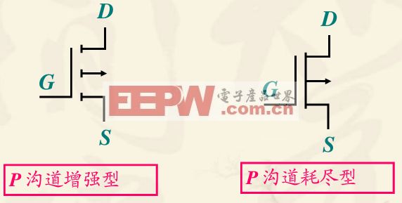
According to the channel material type and the insulated gate type, N-channel and P-channel are divided into two types; according to the conductive mode: the MOS transistor is divided into a depletion type and an enhancement type, so the MOS field effect transistor is divided into an N-channel depletion type and enhancement. Type; P-channel depletion type and enhanced type. 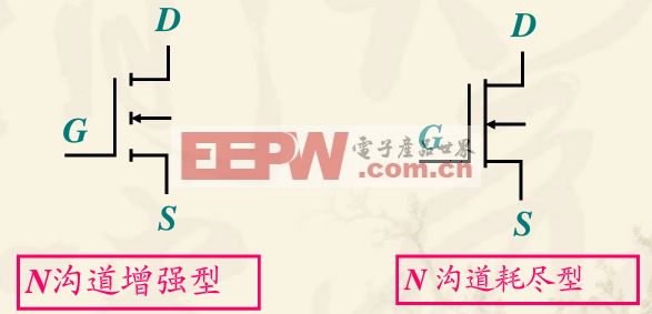
MOS tube application
The most remarkable characteristic of MOS tubes is their good switching characteristics, so they are widely used in circuits that require electronic switches. Commonly used are switching power supplies and motor drives, as well as lighting dimming. Moreover, the CMOS sensor composed of MOS tubes provides a higher and higher image quality for the camera, and has made more "photographers". 
MOS tube working principle - reference materials
1, MOS tube switching loss - flyback analysis
Description: Using flyback analysis of MOS tube switching losses
2, MOSFET works
Description: Structure and operation of a power MOSFET
3. The difference between MOS and triode when used as a switch
Description: The difference between MOS tube and triode used as a switch
Circuit
Cement resistance: is the resistance wire wound on the alkali heat-resistant porcelain, coupled with heat resistant, resistant to wet outside fixed protection and corrosion resistance of the materials and the winding resistance into the square porcelain box body, using special incombustible cement packing seal.The outside of cement resistance is mainly made of ceramic materials (generally divided into high alumina porcelain and feldspar porcelain).
Cement Resistor,Thermal Cement Resistor,Thin Film Cement Resistor,Winding Cement Resistor,Fusing Cement Resistor
YANGZHOU POSITIONING TECH CO., LTD. , https://www.cnfudatech.com