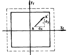
The working process of the lithography machine is as follows: all the fields on the silicon wafer are exposed one by one, that is, stepwise, and then the silicon wafer is replaced until all the silicon wafers are exposed; when the processing of the silicon wafer is finished The mask is replaced, and then the second layer of the pattern is exposed on the silicon wafer, that is, the repeated exposure is performed. Among them, the pattern exposed by the second layer mask must be accurately stacked with the first layer mask exposure, so it is called engraving. As shown in FIG. 1, it is assumed that the dotted frame in the figure is the exposed image of the first mask, and the solid line frame is the second exposed image. In theory, the two layers of graphics should be completely coincident, but in fact due to various systematic errors and accidental errors, the position of the two layers of graphics has deviated, that is, the so-called engraving error [1] .

Figure 1 Casing error analysis [1]
In integrated circuit fabrication, the relative position between the current layer (resist pattern) on the wafer and the reference layer (in-substrate pattern) describes the deviation of the current pattern from the reference pattern along the X and Y directions. This deviation is distributed on the surface of the wafer; it is also a key indicator for monitoring the quality of the lithography process [1]. Ideally, the pattern of the current layer and the reference layer are aligned, ie the overlay error is zero [2].
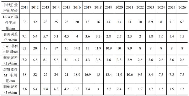
In order to ensure that the design of the upper and lower layers of the circuit can be reliably connected, the alignment deviation between a certain point in the current layer and the corresponding point in the reference layer must be less than 1/3 of the minimum spacing of the figure. The international technology roadmap for semiconductor (ITRS) has set the requirements for the lithography of each technology node, as shown in Table 1. As can be seen from the table, as the technology node advances, the alignment deviation (ie, the engraving error) allowed by the key lithography layer is reduced by about 80%. For example, the set error requirement (|mean|+3σ) of the key layer in the 20 nm node is 8.0 nm [2].
Table 1 Allowed engraving errors for each technology node [2]

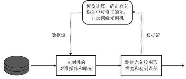
In the lithography process, the engraving error is reduced by the lithography machine alignment system, the splicing error measuring device and the alignment correction software. The work is shown in Figure 2 [2].

Figure 2 Nesting error control system and its data flow [2]
The difference between alignment and overlay error:
Alignment is the process of determining the position of a reference layer pattern on a wafer and adjusting the exposure system to accurately overlap the currently exposed pattern with the pattern on the wafer. The alignment operation is performed by an alignment system in the lithography machine. The engraving error is a parameter to measure the alignment, which directly quantifies the positional deviation between the current layer and the reference layer. The engraving error is measured by a dedicated measuring device [2].
The main causes of the engraving error:
There are many reasons why the exposure pattern is misaligned with the reference pattern. Alignment deviations are introduced by mask deformation or irregularity of the mask, deformation of the wafer itself, distortion of the projection lens system of the lithography machine, and uneven movement of the wafer workpiece stage [2].
references:
[1] Chen Shijie, Research on step-by-step repeating projection lithography machine engraving error model, Micromachining Technology, 1995, 3rd, 8-13
[2] Wei Yayi. Advanced lithography theory and application of VLSI. Beijing: Science Press, 2016.5, 285-285
Lithium Battery Cr17505,3V Lithium Battery,Smoke Detector Batteries,Battery For Smoke Alarm
Jiangmen Hongli Energy Co.ltd , https://www.honglienergy.com