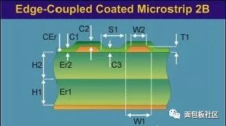
In the high-speed PCB design process, stack design and impedance calculation are the first step in the summit. The impedance calculation method is very mature. The calculation of different software is not much different. It is relatively cumbersome. Some "balanced art" between impedance calculation and process technology is mainly to achieve the purpose of our impedance control, and also to ensure the process. Convenient processing and minimizing processing costs.

Below we summarize some of the considerations for designing stacked impedances to help you improve your computational efficiency.
1. Line width is rather wide, not fine.
Because there are fine limits in the process, there is no limit to the width, so if you adjust the impedance to adjust the line width and hit the limit later, it will be troublesome, either increase the cost or relax the impedance control. Therefore, the relatively wide calculation means that the target impedance is slightly lower. For example, the single-line impedance is 50 ohms. We can calculate 49 ohms. Try not to count 51 ohms.
2. The overall presentation of a trend.
There may be multiple impedance control targets in our design, so the overall is too large or too small, do not appear to be larger than 100 ohms, 90 ohms are too small, such as small and small.
3. Consider the residual copper ratio and the amount of glue.
When the prepreg is etched on one side or both sides, the glue will fill the etched space during the pressing process, so that the thickness of the glue between the two layers will decrease, and the residual copper ratio will be smaller, and the more the filling, the more the remaining less. Therefore, if the required thickness of the two-layer prepreg is 5 mils, a slightly thick prepreg should be selected according to the residual copper ratio.
4. Specify the glass cloth and the amount of glue.
Different glass cloths, different rubber content prepregs or core sheets have different dielectric coefficients, even the almost high level may be the difference between 3.5 and 4, this difference can cause the single line impedance to change about 3 ohms. In addition, the glass fiber effect is closely related to the window opening size. If the design is 10Gbps or higher, and the laminate has no specified material, the board factory uses a single piece of 1080 material, which may cause signal integrity problems.
Of course, the amount of residual copper flow is not accurate. The dielectric coefficient of the new material is sometimes inconsistent with the nominal. Some glass cloth factories do not prepare materials, etc., which will result in the design stack not being realized or the delivery delay. The best way to do this is to let the board factory design the laminate according to our requirements and their experience at the beginning of the design, so that up to a few round trips can get the ideal and achievable stack.
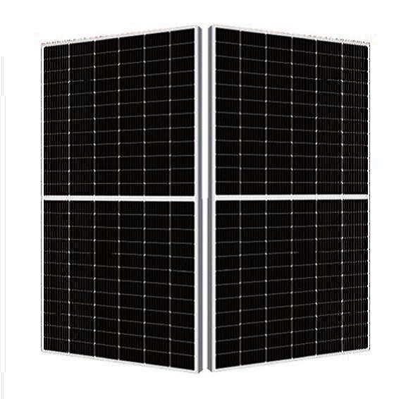
Photovoltaic Monocrystalline Module
The benefits of Solar Panels and solar power is that, once a system has paid for its initial installation costs, the electricity it produces for the remainder of the system's lifespan, which could be as much as 15-20 years depending on the quality of the system, is absolutely free! For grid-tie solar power system owners, the benefits begin from the moment the system comes online, potentially eliminating monthy electric bills or, and this is the best part, actually earning the system's owner additional income from the electric company.

Photovoltaic Monocrystalline Module,Solar Energy Pv Module,Monocrystalline Solar Panel Module,Silicon Pv Mono Solar Module
Jiangxi Huayang New Energy Co.,Ltd , https://www.huayangenergy.com