Basic circuit
Generally, the DC stabilized power supply uses 220 volts as the power supply. After being transformed, rectified, and filtered, it is sent to the voltage regulator for voltage regulation, and finally becomes a stable DC power supply. The transformer, rectification, filtering and other circuits in this process can be regarded as the basic circuit of the DC stabilized power supply. Without these circuits, the regulator circuit will not work normally.
1, transformer circuit
Usually DC regulated power supplies use a power transformer to change the voltage input to the downstream circuit. The power transformer consists of a primary winding, a secondary winding and an iron core. The primary winding is used to input the AC voltage of the power supply, and the secondary winding outputs the required AC voltage. Generally speaking, the power transformer is an electric → magnetic → electrical conversion device. That is, the primary alternating current is converted into a closed alternating magnetic field of the iron core, and the magnetic field of the magnetic field cuts the secondary coil to generate an alternating electromotive force. When the secondary is connected to the load, the circuit is closed and the secondary circuit has an alternating current. The circuit diagram symbol of the transformer is shown in Figure 2-3-1.

2, rectifier circuit
After the transformer is transformed, it is still AC power, which needs to be converted into DC power to be supplied to the rear stage circuit. This conversion circuit is a rectifier circuit. In the DC stabilized power supply, the alternating current of the diode is rectified to direct current by utilizing the single-conductivity characteristic of the diode.
(1) Half-wave rectifier circuit
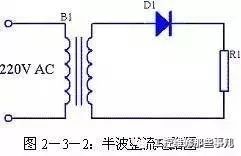
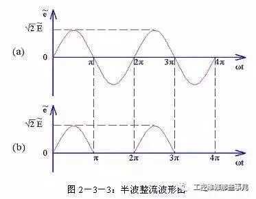
The half-wave rectifier circuit is shown in Figure 2-3-2. Where B1 is the power transformer, D1 is the rectifier diode, and R1 is the load. The B1 secondary is a sinusoidal voltage whose direction and magnitude change with time. The waveform is shown in Figure 2-3-3(a). The period from 0 to π is the positive half cycle of this voltage. At this time, the upper end of B1 is negative at the lower end, the diode D1 is forward-conducting, the power supply voltage is applied to the load R1, and the current flows through the load R1; this period is π~2π The negative half cycle of the voltage, at this time B1 secondary upper end is negative lower end is positive, diode D1 is reversed, no voltage is applied to load R1, no current flows through load R1. The above process is repeated in subsequent cycles of 2π to 3π, 3π to 4π, etc., so that the waveform of the negative half cycle of the power supply is "cut" to obtain a voltage in a single direction, as shown in Figure 2-3-3(b). Since the magnitude of the voltage waveform thus obtained changes with time, we call it pulsating DC.
Let B1 secondary voltage be E. Under ideal conditions, the voltage across load R1 can be obtained by the following formula:

The reverse peak voltage that the rectifier diode D1 is subjected to is:

Since the half-wave rectification circuit only uses the positive half cycle of the power supply, the utilization efficiency of the power supply is very low, so the half-wave rectification circuit is only used in a few cases such as high voltage and small current, and is rarely used in a general power supply circuit.
(2) Full-wave rectifier circuit
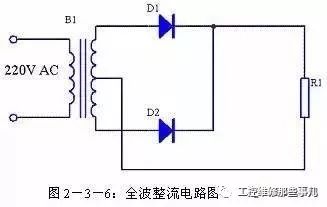
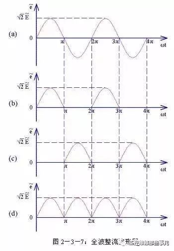
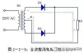
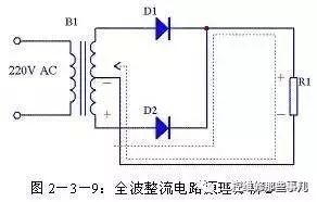
Since the efficiency of the half-wave rectification circuit is low, it is natural to think of using the negative half cycle of the power supply, so that there is a full-wave rectification circuit. The full-wave rectification circuit diagram is shown in Figure 2-3-6. Relative to the half-wave rectification circuit, the full-wave rectification circuit uses a rectifier diode D2, and the secondary of the transformer B1 also adds a center tap. This circuit essentially combines two half-wave rectification circuits. During the period from 0 to π, the secondary upper end of B1 is negative at the lower end, D1 is forward conduction, the power supply voltage is applied to R1, and the upper end of the voltage across R1 is negative at the lower end, and its waveform is shown in Figure 2-3-7(b). As shown, its current flow is shown in Figure 2-3-8; during π~2π, the secondary upper end of B1 is negative and the lower end is positive, D2 is forward-conducting, the power supply voltage is applied to R1, and the voltage across R1 is still at the upper end. The lower end is negative, and its waveform is shown in Figure 2-3-7(c). The current flow is shown in Figure 2-3-9. The above process is repeated in subsequent cycles of 2π~3π, 3π~4π, etc., so that the voltage of the positive and negative power supply for two and a half cycles is rectified by D1 and D2 and respectively added to R1, and the voltage obtained on R1 is always positive and negative. The waveform is shown in Figure 2-3-7(d).
Let B1 secondary voltage be E. Under ideal conditions, the voltage across load R1 can be obtained by the following formula:

The reverse peak voltages experienced by rectifier diodes D1 and D2 are:

The current flowing through each rectifier diode of the full-wave rectifier circuit is only half of the load current, which is twice the half-wave rectification.
(3) Bridge rectifier circuit
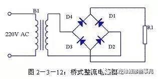
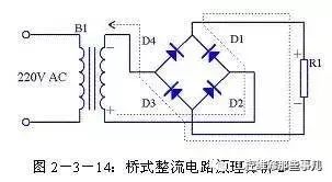
Since the full-wave rectification circuit requires a special transformer, it is troublesome to manufacture, and a bridge rectifier circuit has appeared. This rectifier circuit uses a common transformer, but uses two rectifier diodes more than full-wave rectification. Since the four rectifier diodes are connected in the form of a bridge, the rectifier circuit is called a bridge rectifier circuit.
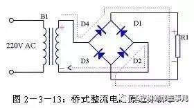
It can be seen from Fig. 2-3-13 that the positive upper end of B1 is positive and the lower end is negative, the rectifier diodes D4 and D2 are turned on, and the current is returned from the secondary upper end of transformer B1 through D4, R1, D2. The lower end of transformer B1; from Figure 2-3-14, it can be seen that in the negative half cycle of the power supply, the lower end of B1 is positive, the upper end is negative, the rectifier diodes D1 and D3 are turned on, and the current is passed from the lower end of transformer B1 to D1. , R1, D3 return to the secondary upper end of transformer B1. The voltage across R1 is always up and down, and its waveform is consistent with full-wave rectification.
Let B1 secondary voltage be E. Under ideal conditions, the voltage across load R1 can be obtained by the following formula:

The reverse peak voltages experienced by rectifier diodes D1 and D2 are:

The current flowing through each rectifier diode of the bridge rectifier circuit is half of the load current, which is the same as full-wave rectification.
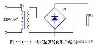
In general, the bridge rectifier circuit is simplified to the form of Figure 2-3-17.
(4) Double voltage rectifier circuit
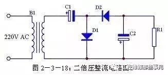
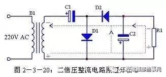
The output voltages of the three rectifier circuits described above are all less than the effective value of the input AC voltage. If the output voltage is greater than the effective value of the input AC voltage, the voltage doubler circuit can be used, as shown in Figure 2-3-18. As shown in Figure 2-3-19, in the positive half cycle of the power supply, the secondary upper end of transformer B1 is negative at the lower end, D1 is turned on, D2 is turned off, C1 is charged through D1, and the voltage across C1 is close to the peak value of B1 secondary voltage after charging. The direction is negative at the right end of the left end; as shown in Figure 2-3-20, in the negative half cycle of the power supply, the secondary upper end of the transformer B1 is positive and the lower end is positive, D1 is cut off, D2 is turned on, C2 is charged through D1, and C2 is charged after charging. The terminal voltage is close to the sum of the voltage across C1 and the peak value of the secondary voltage of B1, and the direction is negative at the upper end of the lower end. Since the load R1 is connected in parallel with C1, when R1 is sufficiently large, the voltage across R1 is approximately twice the B1 secondary voltage.
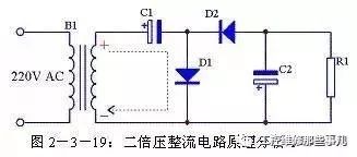
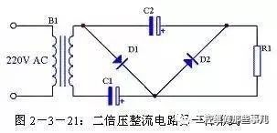
There is another form of drawing for the double voltage rectification circuit, as shown in Figure 2-3-21. The principle is exactly the same as Figure 2-3-18, but the representation is different.
The double voltage circuit can also be easily extended to an n-fold voltage circuit. The specific circuit is shown in Figure 2-3-22.

3, the filter circuit
After the AC power is rectified, a pulsating DC is obtained. Such a DC power supply cannot be directly used as a power source for an electronic circuit because of the large AC ripple. The filter circuit can greatly reduce the AC ripple component and make the rectified voltage waveform smoother.
(1) Capacitor filter circuit
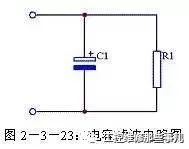
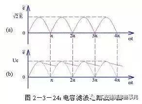
The capacitor filter circuit diagram is shown in Figure 2-3-23. The capacitor filter circuit uses the charge and discharge principle of the capacitor to achieve the filtering effect. In the rising portion of the pulsating DC waveform, the capacitor C1 is charged. Since the charging time constant is small, the charging speed is fast; in the falling portion of the pulsating DC waveform, the capacitor C1 is discharged, and since the discharge time constant is large, the discharging speed is very slow. Charging starts again when C1 has not fully discharged. This achieves filtering by repeated charge and discharge of the capacitor C1. The voltage waveform across the filter capacitor C1 is shown in Figure 2-3-24(b).
When selecting a filter capacitor, the following conditions must be met:

(2) Inductive filter circuit
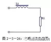
The inductive filter circuit diagram is shown in Figure 2-3-26. The inductive filter circuit uses the inverse electromotive force of the inductor to the pulsating DC to achieve the filtering effect. The larger the inductance, the better the filtering effect. The inductive filter circuit has better load capacity and is often used in applications where the load current is large.
(3) RC filter circuit
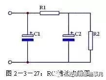
The RC filter circuit is also composed of two capacitors and one resistor, which is also called a π-type RC filter circuit. See Figure 2-3-27. This filter circuit adds a resistor R1 to share the AC ripple on R1. The larger the R1 and C2, the better the filtering effect, but if the R1 is too large, the voltage drop will be too large and the output voltage will be reduced. Generally R1 should be much smaller than R2.
(4) LC filter circuit
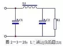
In contrast to the RC filter circuit, there is also an LC filter circuit which combines the advantages of small ripple of the capacitor filter circuit and strong load capacity of the inductor filter circuit. Its circuit diagram is shown in Figure 2-3-28.
(5) Active filter circuit
When the filtering effect is required to be high, the filtering effect can be improved by increasing the capacity of the filtering capacitor. However, due to the capacitance limitation, it is impossible to increase the capacity of the filter capacitor without limitation. In this case, an active filter circuit can be used. The circuit form is shown in Figure 2-3-29, where the resistor R1 is the base biasing resistor of the transistor T1, the capacitor C1 is the base filter capacitor of the transistor T1, and the resistor R2 is the load. This circuit actually amplifies the capacity of C1 by a factor of β by the amplification of the transistor T1, that is, equivalent to a capacitor connected to a (β+1) C1 for filtering.
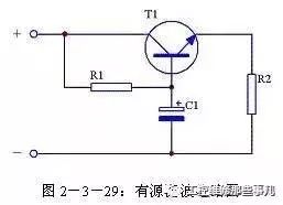
In Figure 2-3-29, C1 can select tens of micro-methods to hundreds of micro-methods; R1 can choose several hundred ohms to several thousand ohms, the specific value can be determined according to the β value of T1, β value is high, R can be taken The value is slightly larger, as long as the collector-emitter voltage (UCE) of T1 is greater than 1.5V. When selecting T1, pay attention to the dissipated power PCM must be greater than UCEI. If the heat is large during operation, the heat sink needs to be added.
The active filter circuit belongs to the secondary filter circuit, and the filter circuit such as capacitor filter should be used in the front stage, otherwise it will not work normally.
4, rectifier filter circuit summary
(1) Comparison of common rectifier circuit performance

Note: U is the voltage value across the load; I is the current value on the load; e is the voltage drop of the rectifier diode, which is generally 0.7V.
(2) Comparison of common passive filter circuit performance

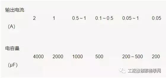
(3) The relationship between the output current of the capacitor filter circuit and the filter capacitance
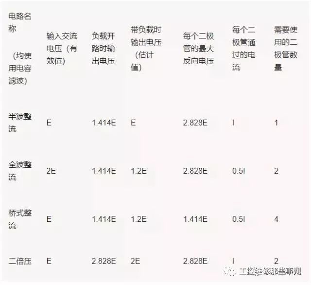
(4) Common rectification and filtering circuit calculation table
Pv Branch Connector,Mc4 Y Type Connector,Mc4 Branch,Mc4 Branch Adapter
Sowell Electric CO., LTD. , https://www.sowellsolar.com