In view of the analysis of the characteristics and main parameters of TVS devices and their working principles, this paper proposes that TVS can effectively protect TN power system, DC power supply, signal line and transistor integrated circuit, etc. It has a wide range of applications, and is safe and reliable. A typical application protection circuit for TVS devices in various circuit designs is presented. When applying, the matching components should be selected for different protection objects and related parameters of the circuit.
Power frequency overvoltage, resonant overvoltage and transient overvoltage in the power grid, including operating overvoltage and lightning overvoltage, these dangerous surge energy can not be discharged or absorbed, and invading the internal circuit of electrical equipment, can affect the electronic equipment Normal operation can even burn the circuit; and the integrated digital circuit is easily interfered by surge voltages such as ESD/EFT (electrostatic discharge/electric fast transient burst), which may cause abnormal operation, crash, and even damage and cause other safety problems. . The use of TVS devices to finely protect the circuit can effectively protect the precision components in the electronic circuit from various surge pulses. This paper is of great significance for the detailed analysis and research of the characteristics and applications of TVS devices.
1 Structure and classification of TVSThe TVS transient voltage suppressor is based on a Zener diode and is a new high-performance protection device in the form of a diode.
TVS usually adopts a diode-type axial lead package structure. The core unit of TVS is a chip. The main material of the chip is semiconductor silicon wafer or drying film. The chip has two kinds of structures: unipolar and bipolar. The monopole TVS has a PN. The junction, bipolar TVS has two PN junctions. The PN junction of the TVS chip is led out by glass purification and is then encapsulated by a modified epoxy resin.
The TVS transient voltage suppressor is unipolar and bipolar. The unipolar only protects against surge voltage surges in one direction, and the bipolar transient diodes strike against opposite polarity surge voltages. The protection function is equivalent to the reverse connection of two Zener tubes. The advantage is that the junction capacitance is small, the response time is short, and the power is large. One-way TVS is mostly used for DC and known direction signal circuits. Bipolar TVS is mostly used for AC and changing signal circuits. TVS arrays are mostly used for multi-line protection. The TVS tube can also be connected in series with the diode. The use of a small parasitic capacitance of the diode reduces the total parasitic capacitance and protects the high-speed signal port. The TVS serial access circuit can be divided into voltages, and parallel access can be divided into currents. However, the serial/parallel number should be controlled in the application. In the application process, the TVS must consider the influence of ambient temperature and temperature changes on the TVS characteristics, because the temperature rises. This will increase the TVS reverse leakage current and reduce power consumption. In addition, TVS can be divided into 500 W, 1 000 W, 1 500 W, 5 000 W and other models according to the peak power.
2 TVS main parameters and selection2.1 Minimum breakdown voltage VBR
The minimum breakdown voltage VBR is equal to the voltage value of the TVS pole when the test current passes through the TVS. VBR is divided into two types according to its degree of dispersion from standard values: VBR (5%) and VBR (10%).
2.2 rated reverse working voltage VWM
When the TVS works in reverse, under the specified IR conditions, the voltage value of the TVS poles is called the rated reverse working voltage VWM. In general, VWM=(0.8~0.9)VBR, the dispersion is 5% TVS, VWM=0.85 VBR (5%); TVS with a dispersion of 10%, VWM = 0.81 VBR (10%). The VWM value should be selected moderately. The VWM value should be greater than or equal to US (maximum continuous operating voltage), and should be close to the US value. If the selection is too large or too small, the circuit cannot be safely and reliably protected.
2.3 Maximum reverse pulse peak current IPP
When the TVS operates in reverse, the maximum peak pulse current allowed by the TVS under the specified pulse conditions is called the maximum reverse pulse peak current, and the peak pulse current IPP should be greater than the circuit transient surge current.
2.4 Maximum clamping voltage VC
When the pulse peak current IPP flows through the TVS, the maximum peak voltage of its two poles is the maximum clamp voltage. VC is the voltage protection level of TVS. It is a key parameter for selecting TVS. It should be less than the UW of the protected circuit. Otherwise, TVS will lose its protection. The TVS clamp factor is equal to VC VBR, and the clamp factor is generally in the range of 1.2 to 1.4.
2.5 Peak Pulse Power Ppp
The peak pulse power is equal to the product of the maximum peak pulse current IPP allowed by the TVS to pass through the maximum clamp voltage VC. The Ppp value is related to the pulse waveform, pulse time, and ambient temperature. In the application, the expected transient surge current and possible transient surge pulse power of the circuit should be determined according to the characteristics of the circuit and the working environment. The peak pulse power Ppp should consider a safety margin of 20%, and the rated pulse power of the TVS is determined accordingly. Pppm. The rated pulse power should be greater than the peak pulse power that may be present in the protected device or line. At the same time, the circuit design must carefully consider the accumulation of repeated applied pulse energy, and its energy should not exceed the pulse energy rating of the TVS device.
2.6 Capacitor C
The capacitance of a TVS is determined by the area of ​​its chip and the bias voltage, and its bias voltage is inversely proportional to the capacitance value C. In the application, the appropriate capacitance range should be selected according to the circuit holding capacity. The capacitor assembly causes the signal to be lost, and the signal is modulated to cause interference.
2.7 Reverse Leakage Current ID
When the rated reverse operating voltage VWM is applied to the TVS poles, the TVS is in the reverse-off state, the current flowing through the TVS is called the reverse leakage current, and the ID value should be less than or equal to its maximum reverse leakage current.
2.8 Clamp response time TC
Clamp response time refers to the time when the TVS pole voltage rises from zero to the minimum breakdown voltage VBR. The TVS TC is less than 1 & TImes; 10-12 s, only 1 ps.
3 TVS characteristics analysis3.1 volt-ampere characteristics of TVS
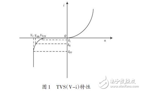
TVS can protect the transistor circuit by clamping the volt-ampere characteristic. See Figure 1. When the TVS tube voltage is reverse biased and located at 0~VBR, the TVS tube is in a high resistance state; when the reverse bias voltage exceeds VBR, The current flowing through the TVS tube increases rapidly, entering a low-resistance conduction state, and the delay from the high-resistance state to the low-resistance state is only ps. The voltage across the TVS tube is clamped below the VC. After the voltage pulse, the TVS tube returns to a high impedance state.
3.2 TVS clamping characteristics
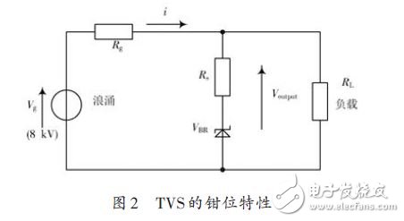
TVS is a voltage-limiting surge protection device that can clamp the overvoltage and limit the surge voltage within the safe withstand voltage range to protect the downstream load circuit. According to the basic theory of the circuit, according to the loop voltage analysis method, it can be seen from Fig. 2 that the output voltage Voutput of the circuit can be obtained by the formula (1):
![]()
If the surge voltage Vg is 8 kV, Rg is 330 Ω, RS is 0.14 Ω, TVS VBR is 6 V, then i ≈ 24 A, then Voutput=10 V from equation (1).
Using the clamping characteristics of the TVS, the 8 kV hazardous surge voltage is reduced to a safe voltage of 10 V. It should be noted that the above circuit should meet the condition of Rg "RS+RLoad" RS.
4.1 TVS application in TN power system
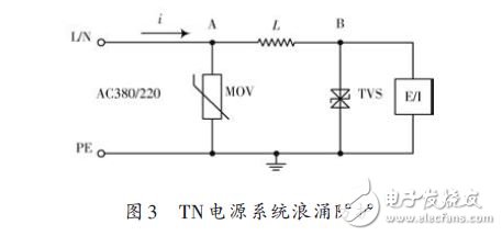
Overvoltages caused by human error such as lightning overvoltage waves and load switches are easily invaded into the interior of electrical and electronic equipment through the power supply line, causing failure or malfunction of electrical and electronic equipment, and even permanent damage to the equipment, causing serious economic losses. Two-stage protection is implemented by installing surge absorbers MOV and TVS on the power line, and common mode and differential mode protection are applied to the L and N lines. The specific method is to install MOV as the first-stage SPD protection at the front end of the line, to amplify part of the lightning current, and install high-power TVS as the second-level SPD protection at the end of the line (device front end) to further weaken the overvoltage amplitude. The grid voltage drops to within the E/I safe withstand voltage range, as shown in Figure 3. It should be noted that the MOV and TVS should achieve the coordination and cooperation of voltage and energy. The length of the line between AB should not be less than 5 m. Otherwise, the line length should be increased or the decoupling device should be installed.
4.2 TVS application in network signal lines
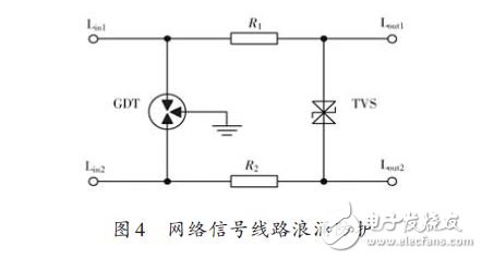
TVS can be used not only for surge protection of power supply systems, but also for surge protection of signal lines. GDT and TVS tubes are combined into a signal surge protector, which is characterized by fast response and small leakage. No loss to the signal, it can provide safe and reliable protection for high-speed network lines, as shown in Figure 4.
4.3 TVS application in DC power system
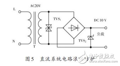
Figure 5 shows the power supply circuit of a common PC computer. The mains AC 220 V is stepped down to AC 20 V through a transformer, and then modulated by a rectifying circuit to output a DC 10 V DC power supply and connected to the load. By installing a bidirectional transient voltage suppressor TVS1 at the output of the transformer, the instantaneous impulse current of the L and N lines is absorbed, and the circuit voltage is clamped at a safe voltage level. The TVS1 can protect the transformer back-end rectifier and other circuit components. A unidirectional transient voltage suppressor TVS2 is installed at the DC power output of the rectifier to protect the DC load from overvoltage current surges.
4.4 TVS application in transistor circuits
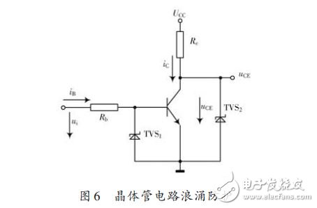
As a current-controlled device, the transistor is an important part of electronic integrated circuits. It can be divided into NPN tube and PNP tube [5], which are applied to switching circuits, amplifier circuits and voltage regulator circuits. In order to protect the transistor circuit from surge voltages such as ESD/EFT (electrostatic discharge/electric fast transient pulse group), TVS1 and TVS2 are added to the input and output terminals of the circuit for protection. The protection circuit is shown in Figure 6. Show.
4.5 Using TVS to protect TTL logic circuits
Is the TTL circuit a transistor? The abbreviation of transistor logic circuit is the most widely used kind of gate circuit. It realizes logic function by inputting high and low level [5]. It consists of three parts, the input stage (emitter transistor V1 and base resistor R1), the inverting stage (V2 tube and resistor R2, R3), and the output stage (V3, V4, V5 and resistor R4, R5). For the surge protection of TTL logic circuit, it is mainly protected by adding TVS1 and TVS2 to the input terminals A and B respectively, adding TVS4 to the output terminal of the circuit for protection, and adding TVS3 for protection at the UCC end of the DC power supply. Effectively suppresses various transient overvoltages from damaging the EB junction or CE junction of the transistor. Figure 7 shows a typical protection circuit for a TTL NAND gate.

4.6 Using TVS to protect MOS integrated circuits
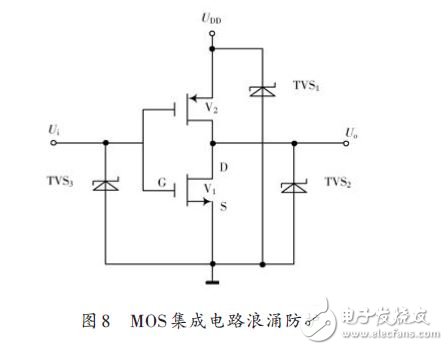
The basic component of the MOS integrated circuit is a MOS transistor. The MOS transistor has three electrodes, a source S, a drain D, and a gate G. It is a voltage control component, and the drain and source currents are controlled by a varying gate-drain voltage. The MOS transistor is divided into P. Two types of MOS tubes and N-type MOS tubes. A complementary MOS circuit composed of an NMOS transistor and a PMOS transistor is called a CMOS circuit, which can provide a fast charge and discharge loop for the capacitance of the output terminal, has low power consumption, high working speed, and has strong load capacity and anti-interference ability. It is getting more and more widely used in digital integrated circuits. Figure 8 is a circuit diagram of the protection circuit of the COMS inverter. The input terminal Ui, the output terminal Uo and the power supply voltage UDD are added to the TVS3, TVS2, and TVS1, respectively, to protect the transistor circuit and the subsequent load components.
(1) TVS has the advantages of fast response, high power, small inter-electrode capacitance and small volume, no leakage current, wide application fields, etc., which can effectively protect TN power system, DC power supply, signal line and transistor integrated circuit, etc. Mode/differential mode surge surges and transient surge voltages such as ESD/EFT.
(2) The circuit design should consider the characteristics of the protected circuit, the working environment and the TVS VC, IPP, VWM, VBR, Ppp and other related parameters to select the adapted TVS protection device. The TVS access circuit should not affect the normal operation of the circuit. It can safely discharge the expected transient surge current and clamp the dangerous voltage within the safe withstand voltage of the circuit.
Custom Made Length 35 cm USB C to iOS Phone Cable Cord, Right Size Angle for DJI Mini 2/3 Pro/Mavic Air 2 / Mavic 3 Remote Controller & iPhone, iPad Devices
Compatible for DJI Mini 2, Maivc 3 pro & Mavic Air 2 Remote Controller,works for iPhone/iPad Device
Perfect length (35cm) and right angle Connecting when you use tablet holder for drones with the devices.
Unique 90 Degree Plug Provides a slim fit in narrow spaces.
This cable can transfer data and charger with all iOS Device
Custom Requirements
In addition to the off the shelf offerings Technical Cable Applications skilled specialists are ready to help with any custom cable assembly requirements you might have. UCOAX stocks cables by the thousands and can custom build anything not on hand. Please contact the UCOAX Technical Sales Team for assistance with all your cable assembly needs.
Drone Cable,Drone Battery Charger Cable,Drone Cables,Drone Controller Cable
UCOAX , https://www.jsucoax.com