Traditional fiber-optic detection systems are mostly based on the MCU architecture. Although the MCU system or DSP processor is powerful in digital signal processing, it is difficult to complete a large amount of real-time data acquisition. The measurement error caused by the small sampling points will accumulate. Test Results. This design is based on the detection principle of fiber optic system and designs a fast fiber inspection system. The data acquisition system uses FPGA for data processing, which enables high-speed real-time data acquisition.
Optical fiber communication is a new communication technology that uses optical fiber as a transmission medium and optical wave as a carrier to realize information transmission, thereby achieving communication purposes. Compared with traditional electrical communication, optical fiber sensing technology has the advantages of high precision and sensitivity, anti-electromagnetic interference, long life, corrosion resistance, low cost, extremely low optical fiber transmission loss, and long transmission distance.
Although fiber optic communication has the above outstanding advantages, its own defects can not be ignored, such as: fiber texture is brittle, easy to break, poor mechanical strength, bending can not be too small; power supply is difficult; shunting, coupling is not flexible; fiber cut And connections require specific tools or equipment. Man-made behaviors such as urban construction, flooding, man-made damage, crustal movement, or damage to natural disasters can easily cause failure of optical fiber lines. How to effectively ensure the reliability of optical fiber communication systems has always been a technical problem to be solved. This design studies the reliability of fiber-optic communication monitoring systems based on fiber-optic communication. The FPGA can replace the traditional MCU architecture to complete data acquisition and processing, and can complete high-speed real-time data acquisition with small measurement error and high operational reliability.
1 Measurement principle of optical fiber communication system
In current fiber measurement, it is mainly to measure the loss and breakpoint of the fiber. The measurement is mainly based on two optical phenomena, Rayleigh scattering and Fresnel reflection. Rayleigh scattering is an inherent property of fiber materials. Due to the diffuse reflection of impurities and core additions contained in the fiber, some of them are backscattered to form Rayleigh backscatter, which is the whole length of the fiber. Fresnel reflections only occur when the fiber is in contact with air or at a joint such as a mechanical joint. Therefore, the measurement of fiber loss is mainly based on the principle of Rayleigh scattering; the main principle based on the measurement of fiber breakpoint is Fresnel reflection.
Rayleigh scattering loss can be approximated by the following formula:

In the formula (1), λ is in units of um, and A and B are constants related to quartz and a doping material.
The signal intensity of Fresnel reflected light is related to the condition of the reflecting surface and the power of the transmitted light. For Fresnel reflected light from the L point on the fiber, the optical power Pf(L) measured at the fiber injection end is:

In the above formula, L is the distance from the Fresnel reflection from the light injection end, R is the power reflection coefficient at L in the fiber, P0 is the peak power of the injected fiber, and β is the fiber attenuation constant.
2 hardware design
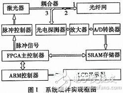
Figure 1 shows the schematic diagram of the system hardware design. The electric pulse generated by the pulser drives the light source module to generate a light pulse, which is injected into the fiber to be tested via the directional coupler. The light pulse injected into the fiber will produce Rayleigh scattered light due to the inherent properties of the fiber material. Fresnel reflected light will be generated together with the end face of the uneven fiber, and will be reflected back to the directional coupler and injected into the photodiode. Electric pulse. The converted electrical signal is sent to the data processing module via the amplifier and A/D conversion processing. Since the reflected light intensity is weak, it needs to be repeatedly transmitted, collected, and amplified and averaged. The OTDR uses its laser source to repeatedly transmit light pulses to the fiber under test to achieve measurement.

2.1 Data Acquisition and Processing Module
The data acquisition and processing module mainly includes the main controller FPGA, AD converter and SRAM memory; mainly completes the collection and processing of real-time data. This design uses FPGA chip for EP3C35Q240C8, there are 240 pins, divided into 8 banks, distributed around the chip, but not all pins can be used at will, only the L/O interface pin is the chip Internally assignable. These interfaces are used to provide reset, ADC chip and SDRAM data storage and control signals.
When a design is complete, the design needs to be downloaded to the FPGA for debugging and application. FPGA has a variety of download configuration modes, this design mainly uses AS mode.
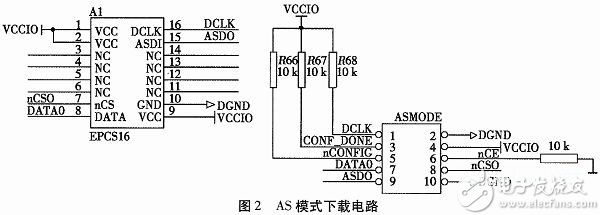
In the AS mode, the download file is first placed in the external load chip. After each power-on, the FPGA automatically calls the load information from the load chip, and then stores it in the SRAM of the FPGA to configure the FPGA. When the design is completed and debugging is correct, this mode should be used to configure the FPGA.
AS download requires an AS configuration chip. The memory used in this design is EPCS16, and its interface with FPGA is 4 signals: DCLK is serial clock input; ASDI is control signal input; nCS is chip select signal; DATA is serial data output. The schematic diagram of the AS mode download circuit implementation is shown in Figure 2.

2.2 Data Transceiver Module
The main function of the data transceiver module is to send an optical pulse signal, which is injected into the fiber to be tested after being coupled by the coupler, and the reflected light reflected by the fiber to be tested is sent to the data acquisition and processing module.
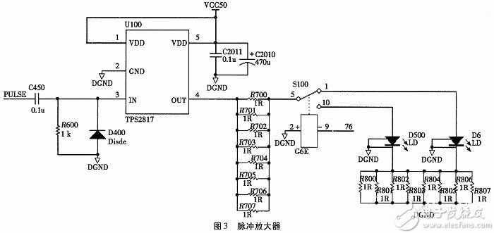
The specific implementation process: First, the FPGA generates a pulse signal, which is amplified by a pulse amplifier, then connected to the photoelectric device, converted into a light pulse of a specific wavelength, and injected into the fiber to be tested, and Rayleigh scattering and Fresnel are generated. The reflection is then sent to the photodetector by the output of the coupler, and the optical signal is converted into an electrical signal, which is then sent to an operational amplifier for amplification and then sent to the data acquisition and processing module. Figure 3 shows the pulse amplifier circuit, which mainly realizes the amplification processing of the pulse signal.

As shown in Figure 3, the TPS2817 is a single-channel high-speed MOSFET driver that can deliver up to 2 A of peak current, up to nanoseconds of switching speed. The input loop includes an active pull-up circuit that uses an open collector to drive the MOS transistor. . The power supply voltage is up to 30 V, and the power supply voltage is at least 2.75 V. When the input pulse signal is connected to the input port IN, the TPS2817 is equivalent to a power driver, and the pulse signal can be power amplified.
3 test results and analysis
First, the detection system emits an optical pulse signal, which is reflected back after encountering the breakpoint, the joint, and the fusion joint. If the detection system can accurately measure the echo time, the distance L can be calculated by the following formula.
Where c is the speed of light, t is the total time from the transmission to the reception of the optical pulse, called the echo time, f is the sampling rate, and N is the total number of sampling points.

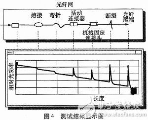
n is the refractive index of the fiber to be tested. The test results are as follows: the abscissa represents the length of the fiber to be tested, and the ordinate represents the relative optical power obtained by measuring the reflected light. The failure of the entire fiber network can be divided into reflective events and non-reflective events.
Melting joints and microbends in the fiber cause losses, but do not cause reflections. On the measurement curve, these two events are expressed in the form of a sudden falling step at the backscatter level. Then the change on the vertical axis is the loss of an event.

Active connectors, mechanical splices, and breaks in the fiber can cause both loss and reflection. The magnitude of the loss is also determined by the amount of change in the back level value. The value of the reflection (usually expressed in terms of return loss) is determined by the magnitude of the reflection peak on the backscatter.
DC meter for solar power multi-channel monitoring. This is a multi-channel power measuring system with LCD display and Modbus RTU communication, available 9 DC channels or 21 channels with an external module provides current, voltage, frequency and bi-directional energy electricity parameters. It`s a perfect measuring component for the renewable power generation industry such as wind power, PV solar power etc.
Dc Multi-Channels Power Meter,Ev Charger Digital Power Meter,Ev Charger Dc Power Meter Multifunctional,Multi-Channel Power Meter For Solar
Jiangsu Sfere Electric Co., Ltd , https://www.elecnova-global.com