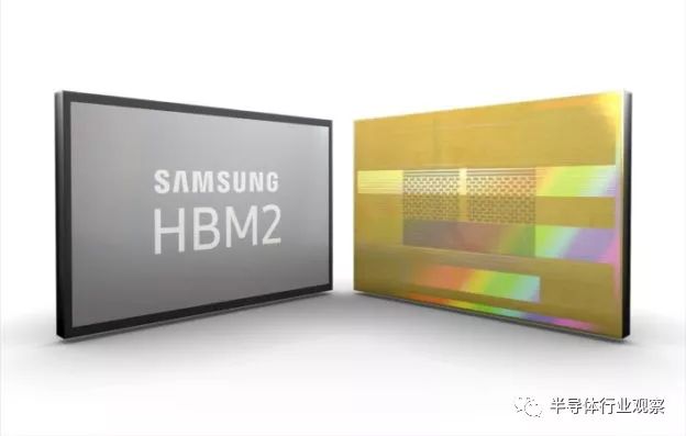
Recently, Samsung Electronics announced that it has begun mass production of its second-generation 8GB high-bandwidth memory-2 (HBM2), the world's fastest data transmission speed, which is the industry's first to provide 2.4Gbps data transmission per pin. Speed ​​of HBM2.
In fact, the development of HBM2 in the past two years can not be rapid. Last year, AMD announced that its Vega graphics card used HBM 2 memory, and finally turned over with these products.
So what is Samsung's bet, what is AMD's HBM2 video memory?

What is HBM?
High-bandwidth memory (HBM) is a high-performance memory interface for 3D stacked DRAMs. It is typically used in conjunction with high-performance graphics accelerators or network devices. It was adopted by JEDEC in 2013 as the industry standard, while the second-generation HBM2 was also in 2016. Month is adopted by JEDEC.
HBM2 is a next-generation memory protocol used in SoC designs to achieve a single pinwidth of 2Gb/s, up to 1024 pins (PIN), and a total bandwidth of 256GB/s (Giga Byte per second). The 1024-pin HBM2 PHY uses a through-silicon via to link to an 8-Hi (8-layer) DDR chip stack. This design requires the use of TSMC's advanced 2.5D package technology, CoWoS. CoWoS uses a sub-micron silicon interface (interposer) to integrate multiple chips into a single package, further improving performance and reducing power consumption to smaller sizes.
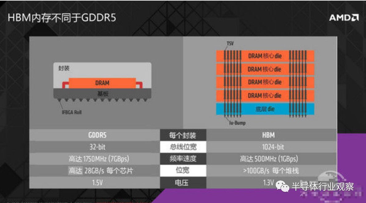
Compared with the traditional GDDR5 memory, HBM is undoubtedly more advanced, and can even be said to be the development trend of high-speed storage in the future! The reason is also very simple. After so many years of development, GDDR5 has come to a bottleneck position. There is not much room for the increase in frequency to provide a larger memory bandwidth, which will inevitably affect the performance of the GPU.

In addition to the specification comparison, this picture can clearly see the actual structure of the HBM, especially the four-layer DRAM stacked on the bottom layer of the bottom die, although AMD has not given the specific fabrication process of the HBM body ( Absolute trade secrets), but it is not difficult to imagine that the 4th layer is by no means the limit of HBM's future development, and as the number of layers increases, the width will surely increase further.
On the contrary, HBM does not need such a high frequency to provide a relatively large memory bandwidth by creating high-bitwidth and low-frequency memory. Under the same 4GB capacity, HBM can provide a memory bandwidth of 4096bit, which is better than GDDR5. 512bit is 8 times higher, which is why HBM can achieve more than GDDR5 memory bandwidth even with only 1GHz equivalent frequency! And this advantage will be further increased with the further improvement of the frequency of HBM memory.
In addition to the performance potential, the actual operating frequency is also related to another very important issue - the higher power consumption brought by higher frequencies, which is the biggest bottleneck of GDDR5. The low operating frequency makes the HBM's watt-up rate three times higher. It is believed that the bit width of the HBM memory will increase with the further increase of the number of layers. At that time, the advantage of low frequency will be further increased. Big!
If you want to say the most important thing in HBM memory technology, then it must be the most basic stack design. Simply put, the traditional 2D circuit design is transformed into a three-dimensional 3D circuit design, making full use of all internal space. I can also greatly reduce the area of ​​the substrate, which also promotes the development of SOC and miniaturization. It can be said that this is an inevitable trend in the development of the semiconductor industry.
What is the advantage of Samsung?
But as we all know, Samsung is not the first to announce the launch of HBM.
Since the first use of HBM memory from the AMD Fiji core, HBM has become the memory standard for the next generation of high-end graphics cards, and HBM 2 is officially listed as the JEDEC standard.
In promoting the development of HBM, in addition to the hard work of AMD, SK Hynix also contributed, but the tragedy is that SK Hynix is ​​blocked by Samsung on HBM 2 memory, AMD Polaris, NVIDIA Pascal high-end graphics card will use Samsung's 4GB HBM2 memory.
Why can you come back later, what advantages does Samsung have?
According to Samsung's official introduction, the new Aquabolt offers the highest level of DRAM performance with a 1.2Gbps pin speed of 1.2V, which is nearly 50% better than the first 8GB HBM2 package. The first generation 8GB HBM2 pin speeds are 1.6Gbps (1.2V) and 2.0Gbps (1.35V) respectively.
Improved, a single Samsung 8GB HBM2 package will provide 307GBps of data bandwidth per second, which is 9.6 times faster than the 8Gb GDDR5 chip with 32GBps of data bandwidth. The four new HBM2 packages in the system will achieve 1.2TBps per second, which will increase overall system performance by up to 50% compared to systems using 1.6Gbps HBM2.
It is reported that in Aquabolt Samsung adopted new technologies related to TSV design and thermal control. An 8GB HBM2 package consists of eight 8Gb HBM2 chips, each with more than 5,000 TSVs for vertical interconnection. Although using so many TSVs can cause parallel clock skew, Samsung has succeeded in minimizing offsets, significantly enhancing chip performance.
In addition, Samsung has increased the number of thermal bumps between HBM2 chips, which makes each package more thermally controlled. Moreover, the new HBM2 has an additional protective layer on the bottom that increases the overall physical strength of the package.
However, Samsung pointed out that because HBM needs to be integrated into ASICs with silicon interposers, this design requires expertise.

The future of HBM2
From the current development situation, HBM technology has developed to the second generation. In addition to AMD, both NVIDIA and Intel have launched related products and applications.
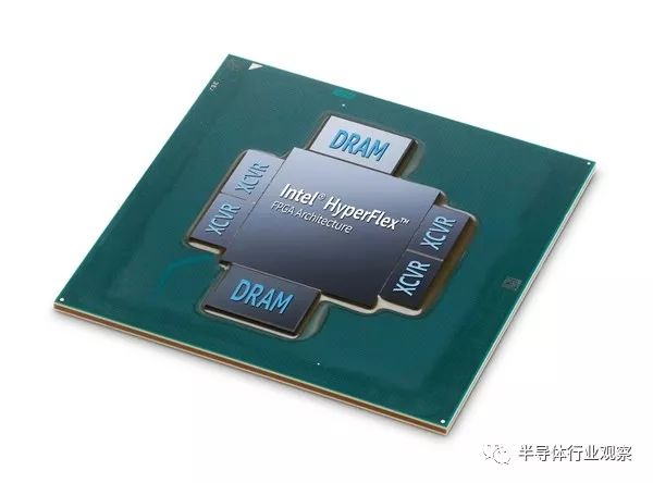
At the end of last year, Intel released the world's first FPGA (Field Programmable Array) chip "Strtix 10 MX" with integrated HBM2 memory, which can provide up to 512GB / s of bandwidth, which is 10 times better than independent DDR2 memory.
At the same time, Samsung also said that its 8GB capacity HBM2 is designed for the next generation of supercomputers, artificial intelligence (AI) and graphics systems, claiming to provide the highest level of DRAM performance.
It is now also possible to see that HBM is being used in some supercomputers, and there will be opportunities to enter standard servers at some point in the future, but it is hard to say what applications will enable HBM to meet high demand for cost reduction.
However, the challenge that this technology needs to overcome is that when production increases and prices decrease, it is difficult to increase production because of the high price at the beginning, which is why HBM2 still mainly appears on high-end graphics cards.
It is also the biggest difficulty for HBM2 to apply to artificial intelligence, high-performance computing and other emerging fields in the future!
Coaxial Car Speakers,15 Coaxial Speaker,15 Inch Coaxial Speaker,Coaxial Speakers Home Audio
Guangzhou Yuehang Audio Technology Co., Ltd , https://www.yhspeakers.com